Copyright © 2006, ZMD AG, Rev. 0.8, 2006-04-12
1/22
All rights reserved. The material contained herein may not be reproduced, adapted, merged, translated, stored, or used without the prior
written consent of the copyright owner. The Information furnished in this publication is preliminary and subject to changes without notice.
ZMD30011
LIN Transceiver
Datasheet
PRELIMINARY
Features
∑
Compliant with LIN Specifications 1.3 and 2.0
∑
Sleep mode and wake-up-function to reduce
power consumption
∑
Wake-up via WAKE-pin, EN-pin, or bus wake-
up-message
∑
Battery related INH pin to control an external
voltage regulator
∑
Interfaces MCU with 3.3V or 5V
∑
LIN bus speed up to 20kBaud
∑
Supply voltage 6.5V to 18V
∑
Operating temperature ≠40 to +125∞C
∑
8kV ESD protection for pins LIN, INH, WAKE,
VSUP
∑
Thermal overload protection
∑
SOP8 package
Benefits
∑
Very low standby current in sleep mode
(typical 14 A)
∑
Excellent electromagnetic compatibility
∑ Bus I/O slew rate control ensures low RF-
emission
Description
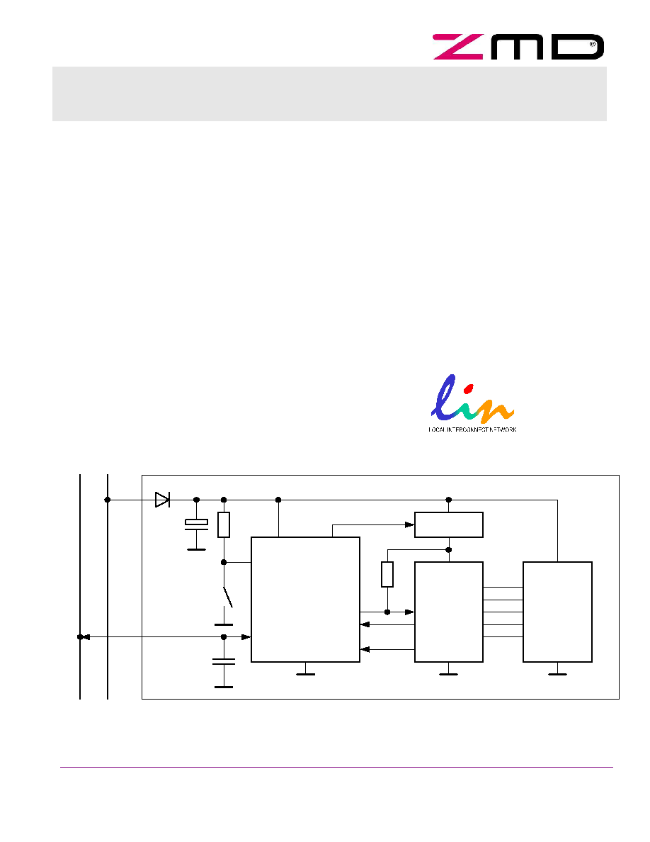
ZMD30011 is a CMOS integrated circuit for
application in a Local Interconnect Network (LIN).
The device is used as a part of a master or slave
node and works as an interface between the
physical bus and the protocol controller.
It realizes data switching (between bus and
TXD/RXD) and level shifting (between battery
voltage and controller voltage).
ZMD30011 is equipped with sleep mode and wake-
up-function to reduce power consumption. It has a
battery related output to control an external voltage
regulator which supplies other devices.
The IC is optimised for automotive environments by
it's very low standby current, excellent
electromagnetic compatibility, ESD protection and
thermal overload protection.
Application Circuit (Example)
ZMD30011
LIN
Transceiver
Voltage
Regulator
Micro-
Controller
RXD
TXD
EN
WAKE
LIN
VSUP
INH
Application
(Sensor,
Actuator,
Switch,
etc)
GND
L
I
N
-
B
u
s
V
B
A
T
Fig. 1: Application Circuit Example

Copyright © 2006, ZMD AG, Rev. 0.8, 2006-04-12
2/22
All rights reserved. The material contained herein may not be reproduced, adapted, merged, translated, stored, or used without the prior written
consent of the copyright owner. The Information furnished in this publication is preliminary and subject to changes without notice.
ZMD30011
LIN Transceiver
Datasheet
PRELIMINARY
Content
1.
BLOCK SCHEMATIC...................................................................................................................................... 3
2.
PIN DESCRIPTION ......................................................................................................................................... 4
2.1
P
IN
C
ONFIGURATION
...................................................................................................................................... 4
2.2
RXD-P
IN
....................................................................................................................................................... 4
2.3
EN-P
IN
.......................................................................................................................................................... 4
2.4
WAKE-P
IN
.................................................................................................................................................... 4
2.5
TXD-P
IN
........................................................................................................................................................ 5
2.6
GND-P
IN
....................................................................................................................................................... 5
2.7
LIN-B
US
-P
IN
.................................................................................................................................................. 5
2.8
VSUP-P
IN
..................................................................................................................................................... 5
2.9
INH-P
IN
......................................................................................................................................................... 6
3.
FUNCTIONAL DESCRIPTION ........................................................................................................................ 7
3.1
S
EQUENCE
C
ONTROL
..................................................................................................................................... 7
3.2
W
AKE
-U
P
-E
VENTS
......................................................................................................................................... 7
3.3
I
NTERNAL
V
OLTAGE
R
EGULATOR
.................................................................................................................... 8
3.4
B
ATTERY
V
OLTAGE
C
ONTROL
......................................................................................................................... 8
3.5
3.3V
AND
5V L
OGIC
C
APABILITY
..................................................................................................................... 8
4.
ELECTROMAGNETIC COMPATIBILITY AND SHORT-CIRCUIT IMMUNITY ............................................ 10
5.
FAIL-SAFE-FEATURES ................................................................................................................................ 10
6.
ELECTRICAL PARAMETERS ...................................................................................................................... 11
6.1
M
AXIMUM
R
ATINGS
...................................................................................................................................... 11
6.2
E
LECTRICAL
C
HARACTERISTICS
.................................................................................................................... 12
7.
TIMING CHARACTERISTICS ....................................................................................................................... 15
8.
PACKAGE ..................................................................................................................................................... 21
9.
RELATED DOCUMENTS.............................................................................................................................. 22
10.
ORDERING INFORMATION ......................................................................................................................... 22
Copyright © 2006, ZMD AG, Rev. 0.8, 2006-04-12
3/22
All rights reserved. The material contained herein may not be reproduced, adapted, merged, translated, stored, or used without the prior written
consent of the copyright owner. The Information furnished in this publication is preliminary and subject to changes without notice.
ZMD30011
LIN Transceiver
Datasheet
PRELIMINARY
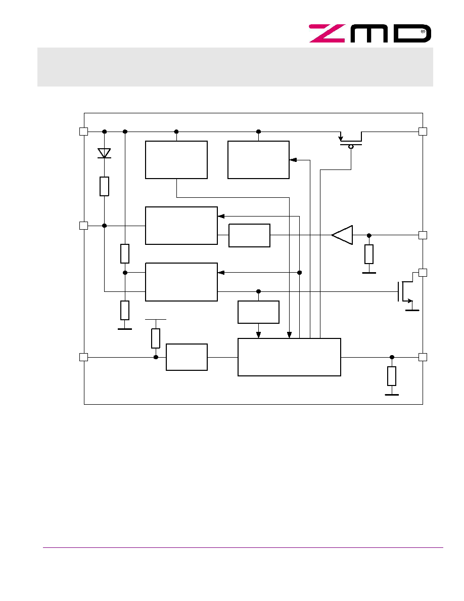
1. Block Schematic
Supply-
Comparator,
POC
Supply
5V
Transmitter
Current Limiter
Slope Control
Receiver
Comparator
Filter
Wake-up
filter
Wake-up
filter
Mode
Control
VSUP
INH
TXD
RXD
EN
VSUP
LIN
WAKE
Time-out
filter
Fig. 2: Block Schematic
Copyright © 2006, ZMD AG, Rev. 0.8, 2006-04-12
4/22
All rights reserved. The material contained herein may not be reproduced, adapted, merged, translated, stored, or used without the prior written
consent of the copyright owner. The Information furnished in this publication is preliminary and subject to changes without notice.
ZMD30011
LIN Transceiver
Datasheet
PRELIMINARY
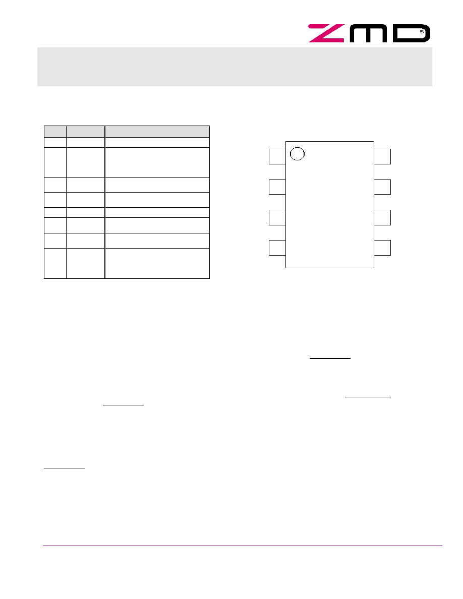
2. Pin Description
2.1
Pin Configuration
PIN
Symbol
Description
1
RXD
receive data output
2
EN
sleep control input
normal mode=high
sleep mode=low
3
WAKE
local wake-up input
4
TXD
transmit data input
5
GND
ground
6
LIN
single wire bus input/output
7
VSUP
battery supply input
8
INH
battery related inhibit output
to control an external voltage
regulator
Fig. 3: Pin Configuration
2.2
RXD-Pin
This pin reports the state of the LIN bus voltage to the protocol controller. A LIN-low-level (dominant state) is
transmitted as a CMOS-low-level. A recessive LIN-state (LIN-high-level) is transmitted as a CMOS-high-level.
The RXD output structure is an open-drain output stage. This allows the ZMD30011 to be used with 3.3 V or 5 V I/O
protocol controllers. If the controller's RXD pin does not have an integrated pull-up, an external pull-up resistor to
the microcontroller I/O supply voltage is required. The driver is tristated in the sleep-mode.
2.3
EN-Pin
This input determines the operation mode of the device. EN=high sets the device to the normal-mode, EN=low sets
the device to the sleep-mode significantly reducing the current consumption.
If the signal is floating then the EN-pin is held on low by an internal pull-down-resistor. The pull-down-current is
restricted to 25 A typically.
2.4
WAKE-Pin
The wake-pin is a high-voltage-input. A low-signal from the system (trigger) wakes up the transceiver from the
sleep-mode (local wake-up). An input filter prevents unintended wake-up in the case of transients. An internal pull-
up-resistor prevents floating of the pin in the unconnected state.
If the application does not require a local wake-up than the wake-pin has to be connected with VSUP.
1
2
3
4
8
7
6
5
SOP8
150 mil
top view

Copyright © 2006, ZMD AG, Rev. 0.8, 2006-04-12
5/22
All rights reserved. The material contained herein may not be reproduced, adapted, merged, translated, stored, or used without the prior written
consent of the copyright owner. The Information furnished in this publication is preliminary and subject to changes without notice.
ZMD30011
LIN Transceiver
Datasheet
PRELIMINARY
2.5
TXD-Pin
This CMOS-input connects the external protocol controller to the transceiver. A TXD-low-level is transmitted as a
LIN-low-level too. The LIN-driver is tristated if TXD is high, hence the bus is set to recessive state using the pull-up-
resistor.
The TXD-input is equipped with an internal pull-down resistor and an internal timer preventing the LIN-bus from
being permanently driven in the dominant state.
2.6
GND-Pin
The GND-pin represents the ground level. Level suspensions 2 V do not influence the data transfer. A ground loss
in the recessive state does not lead to a significant current at the LIN-pin.
2.7
LIN-Bus-Pin
The circuit blocks receiver and transmitter realize the bi-directional LIN-bus-connection.
Receiver:
The input voltage of the receiver depends on the supply voltage ratiometricly. The threshold amounts to 0.4
respective 0.6 VSUP with a typical hysteresis of 10 % VSUP. The receiver is active in the sleep mode too. The filter
in the input signal path suppresses spikes with a duration of < 4 s.
Transmitter:
The transmitter consists of a low-side-driver supplying 20 mA at a typical output-voltage of 1 V.
It transmits a low level if there is a low level on the TXD-pin. An internal pull-up resistor of 30 k pushes the bus
node to the high level in the locked transmitter state.
A diode is located in series to the resistor and prevents a reflow current from the bus into the battery supply line in
the case of a local supply loss or a ground level shift.
The transmitter is only active in the normal-mode. In the sleep-mode and in the wait-mode the transmitter is
tristated. A slope-control adjusts both edges (falling edge from the recessive to the dominant driver state and rising
edge from the dominant to the recessive driver state) to 2V/µs typically. As a result the electromagnetic emission is
minimal.
The capacitive LIN-bus-load has to be restricted to a total of <=10 nF at a total resistance 0.5 k in order to ensure
the symmetry of both edges.
In the case of short circuits to battery supply the drivers current limitation begins to work at 180 mA typical. The
driver is also protected against thermal overloads.
In the range from -18 V to 30 V the current VSUP-LIN is determined only by the pull-up-resistor. A VSUP loss in the
recessive driver state does not lead to a significant current at the LIN-pin.
2.8
VSUP-Pin
The VSUP-pin has to be protected by an external diode against reverse polarity of the battery supply.
The protection against galvanic and capacitive coupled transients is realized by a special internal circuitry.
The operational supply voltage reaches from 6.5 to 18 V DC. A voltage control prevents an incorrect bus transfer
below the operating voltage range.
The quiescent current in the sleep-mode amounts to typical 14 A. In the normal-mode the quiescent current
amounts to max. 2 mA in the state of dominant LIN-bus.