 | –≠–ª–µ–∫—Ç—Ä–æ–Ω–Ω—ã–π –∫–æ–º–ø–æ–Ω–µ–Ω—Ç: CDRM622 | –°–∫–∞—á–∞—Ç—å:  PDF PDF  ZIP ZIP |

Data Sheet
June 1999
CDRM622
622 Mbits/s Multichannel Digital Timing Recovery
Features
s
Receives scrambled serial data at STS-12/STM-4
(622.08 Mbits/s) rate.
s
Demultiplexes serial data to 77.76 Mbytes/s paral-
lel byte wide data with aligned 77.76 MHz clock.
s
Synthesizes 622.06 MHz clock with on-chip PLL,
requiring only 77.76 MHz input reference clock and
one external resistor.
s
Multiplexes parallel 77.76 Mbytes/s data to
622 Mbits/s serial data for transmission.
s
Incorporates n = 1 to 16 channels with modular
design. Implemented in Lucent Technologies
Microelectronics Group HL250C technology.
s
Meets type B jitter tolerance specification of ITU-T
Recommendation G.958.
s
Sources stable clock in absence of data transitions
once the clock synthesizer has acquired lock.
s
Uses single, low-voltage (3.3 V ± 5%) supply.
s
Includes built-in test circuitry such as high-speed
loopback of transmit data into receiver.
s
IDDQ compatible.
s
Powers down the receiver on per-channel basis.
s
Allows JTAG access to high-speed data paths.
Description
The CDRM622 provides a physical medium for high-
speed asynchronous serial data transfer between
ASIC devices. Devices can be on the same PC-
board, or on separate boards connected across a
backplane, or connected by cables. The macrocell is
intended for, but not limited to, terminal equipment in
SONET/SDH and ATM systems.
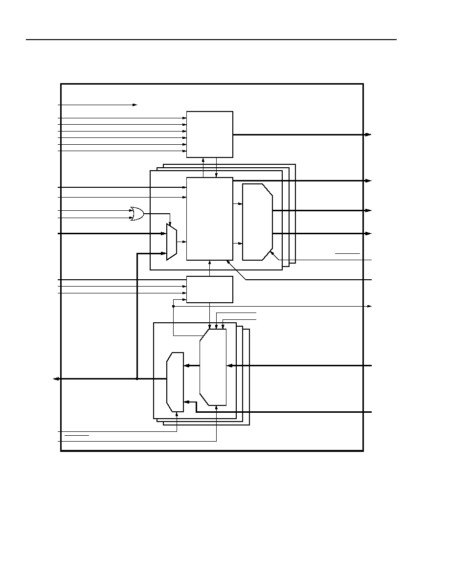
The macrocell consists of three functional blocks.
The receiver accepts 622.08 Mbits/s serial data.
Based on data transitions, the receiver selects an
appropriate 622 MHz clock phase for each channel
to retime the data, then demultiplexes down to
77.76 Mbytes/s parallel bytes and a 77.76 MHz clock.
The transmitter operates in the reverse direction.
77.76 Mbytes/s parallel bytes are multiplexed up to
662.08 Mbits/s serial data for off-chip communica-
tion.
The clock synthesizer generates the necessary
622.08 MHz clock for operation from a 77.76 MHz
reference. Figure 1 illustrates the function of the mac-
rocell.
The hard macrocell can be supplied for up to 16 data
channels. Multiple macrocells can be used on a sin-
gle device. The macrocell is intended to be used with
high-speed differential I/O buffers for the 622 Mbits/s
serial data streams and the 77.76 MHz reference
clock. Common selections are low-voltage differential
swing (LVDS) or PECL. The I/O buffers are part of
our standard-cell ASIC library and are not included in
the macrocell to allow for flexibility.
CDRM622
Data Sheet
622 Mbits/s Multichannel Digital Timing Recovery Macrocell
June 1999
2
Lucent Technologies Inc.
Description
(continued)
5-5833 (F).br.2
Figure 1. CDRM622 Block Diagram
TSTMODE
TSTSHFTLD
BUILT-IN
Rx
CDR
S
E
RIAL
T
O
PARRAL
L
E
L
(
622
Mb
i
t
s/s
TO
78
Mby
t
es/s
)
DEM
U
X
SEL
E
C
T
622.08 MHz
TEST
CLOCK/DATA
ALIGNMENT
SYNTHESIZER
PLL
PARRAL
L
E
L
TO
SERI
A
L
(
7
8
Mb
y
t
es
/
s
TO
62
2 M
b
i
t
s
/
s
)
MU
X
B
O
UNDARY SCA
N
LOOPBKCH[(n ≠ 1):0]
LD[(n ≠ 1):0]R[7:0]
MRESET
(MASTER RESET)
ECSEL
EXDNUP
ETOGGLE
TSTPHASE
TSTCLK
BYPASS
LOOPBKEN
HDIN[(n ≠ 1):0]
622 Mbits/s DATA
REXT
PLLPWRDN
REF78
77.76 MHz
HDOUT[(n ≠1):0]
622 Mbits/s DATA
BSCANEN
RESETTN
(TEST)
TSTMUX[8:0]
BSIPAD[(n ≠ 1):0]
LCKR[(n ≠ 1):0]
RESETRN
TSTCLK
BYPASS
(TEST)
RXPWRDN[(n ≠ 1):0]
LCK78
77.76 MHz
77.76 Mbytes/s
LDAT[(n ≠ 1):0] X[7:0]
BSOPAD[(n ≠ 1):0]
(BOUNDARY SCAN)
1
2
n
Tx
1
2
n
(BOUNDARY SCAN)
77.76 MHz
77.76 Mbytes/s
RETIME

Data Sheet
CDRM622
June 1999
622 Mbits/s Multichannel Digital Timing Recovery Macrocell
3
Lucent Technologies Inc.
Description
(continued)
Physical Size
The macrocell is able to support up to 16 channels of serial data; however, the physical design will be limited to two
sizes (8 and 16). Unused receivers will be powered down for specific applications as the physical size of the mac-
rocell does not vary directly with channels. The physical dimensions of a 16-channel macrocell are approximately
square at 2.2 mm per side.
Power Dissipation
At 3.3 V, power is estimated by 300 mW + 50 mW per Rx channel + 10 mW per Tx channel.
Device IO Buffers
Device IO buffers are not part of the hard macrocell. This allows customers to choose the most appropriate inter-
face levels without disturbing the macrocell. Common choices of device interface levels are LVDS (low-voltage dif-
ferential swing) and PECL. Device pinout is also flexible. Appropriate buffering will be added to the device by
Lucent Technologies Microelectronics Group to ensure data integrity between the IO buffers and the macrocell.

CDRM622
Data Sheet
622 Mbits/s Multichannel Digital Timing Recovery Macrocell
June 1999
4
Lucent Technologies Inc.
Hardware Interface
Low-Speed 77.76 Mbytes/s Interface
The internal timing performance of the macrocell is independent of the remaining device logic with the exception of
the low-speed interface. The macrocell sources clock and data bytes for each channel to be captured and pro-
cessed by the device logic. In the other direction, the device logic sources data bytes to be captured and processed
by the macrocell. These interfaces are generally designed and verified using static timing analysis. Figure 2 illus-
trates these interfaces and their associated timing.
Input Capacitance
For all digital inputs, the input capacitance at the boundary of the macrocell is 0.02 pF.
Output Signal Drive Strength
For all low-speed outputs, the output driver strength is equivalent to that of a Lucent-type SBNS standard cell. (See
HL250C 3.3 Volt 0.25 µm CMOS Standard-Cell Library
, System ASIC Data Book March 1998 (MN97-066ASIC)).
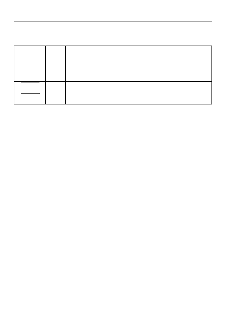
Table 1. Functional Signals
Signal Name
Type
Description
HDIN[(n ≠ 1):0]
I
622.08 Mbits/s serial data inputs. One input for each independent data channel.
LD[(n ≠ 1):0]R[7:0]
O
Low-speed demultiplexed data bytes retimed to recovered 77.76 MHz clocks.
LCKR[(n ≠ 1):0]
O
Low-speed 77.76 MHz recovered clocks.
LCK78
O
Low-speed (77.76 MHz) PLL divide-down clock. Can be used as a PLL activity
monitor point. This buffered version of internal transmit 77.76 MHz clock can be
used to time data transfer into the transmitter.
LDAT[(n ≠ 1):0]X[7:0]
I
77.76 MHz data byte inputs to transmitter.
HDOUT[(n ≠ 1):0]
O
622.08 Mbits/s serial data outputs.
REF78
I
77.76 MHz reference clock input to clock synthesizer.
REXT
I
Connects to external 10 k
±
1% resistor that is tied to ground potential (V
SSA
)
on the circuit pack. Provides reference current to on-chip PLL.
MRESET
I
(Active-High). Asynchronous master reset for macrocell initialization. Also used
in test mode to reset test circuitry.
PLLPWRDN
I
(Active-High). PLL powerdown for I
DDQ
testing.
RXPWRDN[(n ≠ 1):0]
I
(Active-High). Per-channel powerdown of receiver.
Data Sheet
CDRM622
June 1999
622 Mbits/s Multichannel Digital Timing Recovery Macrocell
5
Lucent Technologies Inc.
Hardware Interface
(continued)
5-7714(F)r.2
Figure 2. 78 MHz Interfaces
CLOCK SYNTHESIZER
PHASE
ERROR
DETECTOR
OUTPUT DATA
RELATIVE TO OUTPUT CLOCK
±1.0 ns
16 P
H
AS
E
622
RECEIVER
CK/8
byte
78 MHz
STDCELLS
(TEST LOGIC)
D
S
S
Q
INVERT CLOCK
TO USE
POSITIVE EDGE
FLIP-FLOP
Q
S
S
D
CK/8
78 MHz
REF78
LCK78
byte
TRANSMITTER
622 MHz
INPUT DATA SETUP/HOLD
1.9 ns/0.2 ns
78
MHz
CDRM622
PLL REFERENCE
CLOCK
CDRM622
Data Sheet
622 Mbits/s Multichannel Digital Timing Recovery Macrocell
June 1999
6
Lucent Technologies Inc.
Simulation Interface
PLL Bypass
Device simulating, debugging, and testing with a working PLL is not recommended. Therefore, a test mode that
bypasses the PLL is provided. Functional simulation and factory testing can make use of this mode. The logic of
the data paths remain functional. Only the 622.08 MHz clock source is changed to the test clock. For factory test-
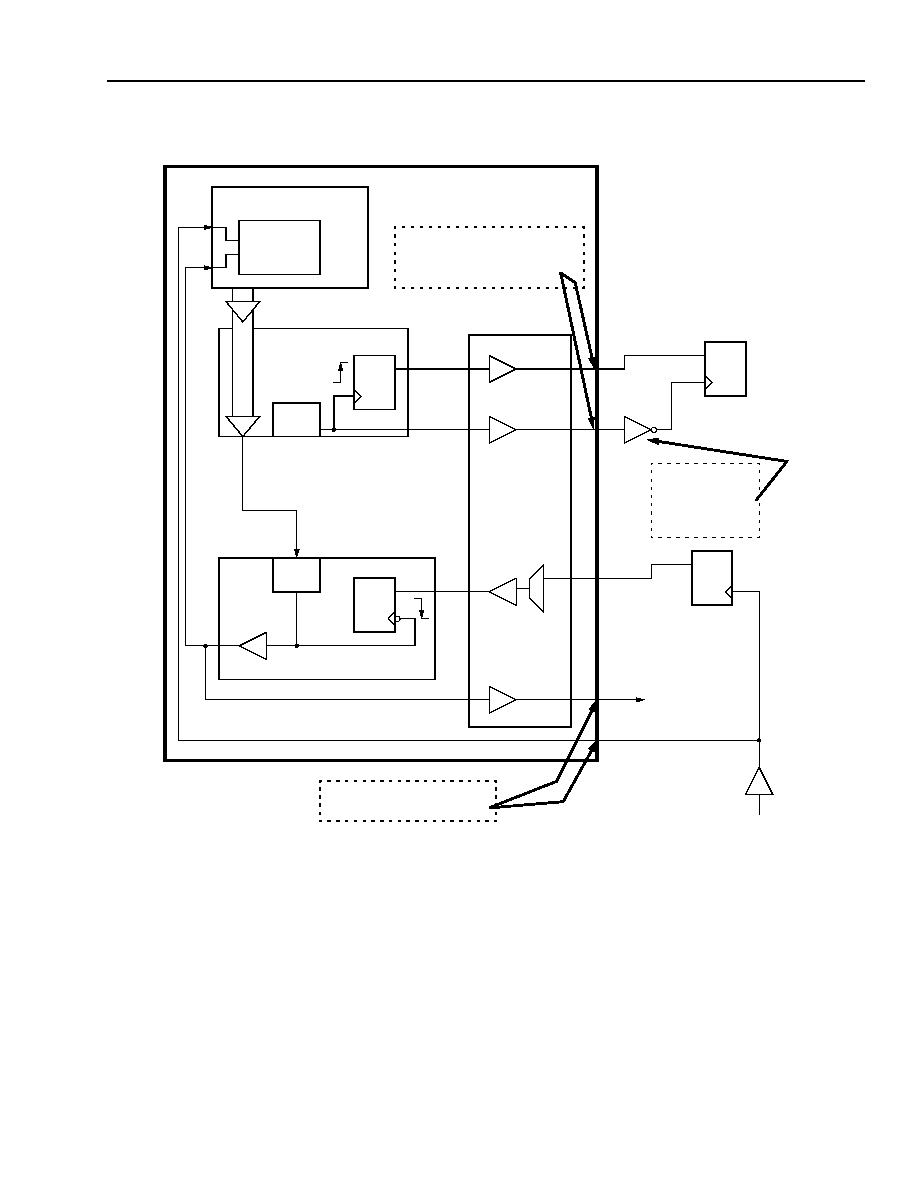
ing, the PLL is separately exercised and monitored through the test port. Figure 3 illustrates this mode.
Logical Timing
Figure 4 and Figure 5 illustrate the functional timing relationships during PLL bypass mode operation.
Internal Clock Synchronization
When the PLL is bypassed, the internal clock dividers are not automatically aligned with the phase of the input ref-
erence clock. Resets are provided as an aid to force a relationship. During PLL bypass, the clock dividers are
clocked by the test clock. The first falling edge of the test clock after the resets become inactive will generate a ris-
ing edge of the internal 77.76 MHz clocks. PLL bypass simulation test benches should be designed so that the
device input signals driving TSTCLK, REF78, RESETRN, and RESETTN are sequenced to closely align the inter-
nal clocks with the reference clock. Figure 6 illustrates this sequence.
Table 2. Simulation Signals
Signal Name
Type
Description
BYPASS
I
(Active-High). Enables functional bypassing of the 622 MHz clock synthesis with
TSTCLK. Receiver and transmitter pass data in a logically correct manner based on
the test clock timing.
TSTCLK
I
Test clock for emulation of 622.08 MHz clock during PLL bypass. This input can run
up to 155 MHz for factory testing. Also used for low-speed fault coverage testing.
RESETTN
I
(Active-Low). Resets transmitter clock division counter to enable synchronizing the
internal 77.76 MHz clock to the reference clock during PLL bypass.
RESETRN
I
(Active-Low). Resets receiver clock division counter to enable synchronizing the
recovered 77.76 MHz clocks to the reference clock during PLL bypass.

Data Sheet
CDRM622
June 1999
622 Mbits/s Multichannel Digital Timing Recovery Macrocell
7
Lucent Technologies Inc.
Simulation Interface
(continued)
5-5834(F).dr.1
Figure 3. PLL Bypass Mode Block Diagram
SE
LECT
LOOPBKCH[(n ≠ 1):0]
HDIN[(n ≠ 1):0]
TSTCLK
LCK78
LDAT[(n ≠ 1):0]X[7:0]
LCKR[(n ≠ 1):0]
LD[(n ≠ 1):0]R[7:0]
BSIPAD[(n ≠ 1):0]
BSCANEN
HDOUT[(n ≠ 1):0]
CDR
(TSTCLK DIVIDE BY 8)
CLOCK/DATA
ALIGNMENT
RETIME
P
A
RA
LLEL T
O
SE
RI
A
L
(78
Mb
yt
es
/
s
T
O
622
Mbits/s)
MU
X
LOOPBKEN
BYPASS (= 1)
SE
RIAL T
O
P
A
RA
LLEL
(6
22 M
bit
s/s
T
O
78 M
b
y
t
es
/
s
)
DEM
U
X
B
O
UND
AR
Y SCA
N
RESETRN
RESETTN
BSOPAD[(n ≠ 1):0]

CDRM622
Data Sheet
622 Mbits/s Multichannel Digital Timing Recovery Macrocell
June 1999
8
Lucent Technologies Inc.
Simulation Interface
(continued)
5-5836 (F).d
Figure 4. 622.08 Mbits/s Receive (PLL Bypass Mode) Timing
5-5837 (F).b
Figure 5. 622.08 Mbits/s Transmit (PLL Bypass Mode) Timing
LSB MSB
MSB
LSB MSB
LSB MSB
LSB
TSTCLK
HDIN[(n ≠ 1):0]
LCKR[(n ≠ 1):0]
LD[(n ≠ 1):0]R[7:0]
0
1
2
3
4
5
6
7
8
9 10 11 12 13
00
8A
59
E4
0
1
2
3
4
5
6
7
8
9 10 11 12 13
LCK78
LDAT[(n ≠ 1)X[7:0]
TSTCLK
HDOUT[(n ≠ 1):0]
E5
C9
8A
BF
FAST
SLOW
GATE DELAYS
MSB
LSB

Data Sheet
CDRM622
June 1999
622 Mbits/s Multichannel Digital Timing Recovery Macrocell
9
Lucent Technologies Inc.
Simulation Interface
(continued)
5-5838 (F).er.1
Notes:
During PLL BYPASS mode, TSTCLK is asynchronous to the REF78 input of the CDRM622; therefore, test resets (RESETTN and RESETRN)
were added to allow establishing a relationship between the internally generated 77.76 MHz clocks and the reference clocks.
RESETRN allows synchronization of the 77.76 MHz recovered clocks in the receiver.
RESETTN allows synchronization of the 77.76 MHz clock internal to the transmitter.
TSTCLK should be stopped high while the resets change but needs to toggle at least four clock cycles while resets are active.
Figure 6. Synchronization of CDRM622 Generated Clocks During Bypass Mode
Test Interface
Boundary Scan
In order to avoid loading the high-speed data signals unnecessarily, access has been provided through the macro-
cell. The state of the input pads can be monitored at buffered test outputs. The state of the output pads can be con-
trolled through a multiplexer built into the macrocell data path.
Table 3. System Test Signals
Signal Name
Type
Description
BSIPAD[(n ≠ 1):0]
O
Provides buffered monitor points reflecting state of the 622.08 Mbits/s device
input pads for use in boundary scan.
BSOPAD[(n ≠ 1):0]
I
Provides access to 622.08 Mbits/s output pads for boundary scan. Output
boundary-scan multiplexers are built into the macrocell.
BSCANEN
I
(Active-High). Enables boundary-scan values to control 622.08 MHz output
device pins.
LOOPBKEN
I
(Active-High). Enables 622.08 Mbits/s loopback mode. All transmit outputs are
directed into the receivers. Overrides individual channel loopback controls.
LOOPBKCH[(n ≠ 1):0]
I
(Active-High). Enables 622.08 Mbits/s loopback mode on a per-channel basis.
8A
96
E4
LD[(n ≠ 1):0]X[7:0]
HDOUT[(n ≠ 1):0]
TSTCLK
REF78
RESETTN
LCKR[(n ≠ 1):0]
TSTCLK STOPPED FOR A MINIMUM OF TEN CLOCK CYCLES
LCK78
RESETRN

CDRM622
Data Sheet
622 Mbits/s Multichannel Digital Timing Recovery Macrocell
June 1999
10
Lucent Technologies Inc.
Test Interface
(continued)
High-Speed Loopback
The output of the transmitter can be looped back into the receiver. This feature enables factory testing 622 Mbits/s
circuitry on a test set only capable of 200 MHz clocking. System product diagnostics may also find a use for this
mode. The loopback function can be selected on a per-channel basis or by a global override.
CDR Testing
Built-in test cirtuitry is included as part of the macrocell in order to ensure quality of manufacture. Test access and
control has been added to facilitate characterization and evaluation of the macrocell function. Macrocell testing is
added by Lucent to verify PLL, high-speed data paths, and fault coverage within the macrocell.
One such test configures the macrocell in high-speed loopback with transmit pattern generation and receive byte
alignment in order to observe 77.76 Mbytes/s data after passing through both transmitter and receiver at
622.08 Mbits/s. This test requires only the PLL reference clock to be sourced from the factory test set.
Also, each of the recovered channels (clock and data byte) can be brought out through the test port one channel at
a time, and the synthesized clock, divided by eight, is brought out for frequency measurement and evaluation.
Macrocell testing is set up by an internal control register that is written through a 3-pin serial test interface.
Built-in testing cannot verify the 78 MHz interface connections to the device logic. Therefore, at least one test exer-
cising the functional data path through the macrocell using PLL bypass is required from the device logic designers.
Test Access
In order to accomplish these tests, access is required to approximately 20 test signals through the device pins. Test
pins can be multiplexed with other pins and TSTMODE = 1 can be used as an indication when CDR test access is
needed. In addition, to standard manufacture testing, access to built-in test features has been useful during func-
tional board-level prototype prove-in.
CDR testing requires access to the following signals from the device pins: TSTMODE, BYPASS, TSTCLK,
RESETRN, RESETTN, TSTSHFTLD, ECSEL, EXDNUP, ETOGGLE, LOOPBKEN, TSTPHASE, TSTMUX[8:0].
REF78, MRESET, and HDIN[(n ≠ 1):0] are also used during testing but are expected to be controllable through
functional device pins. REF78 should be controllable through the reference clock input to the device. A 155 MHz
reference clock pin which is divided on-chip to 78 MHz is acceptable. MRESET should be controllable through the
device powerup reset pin.
Table 4. CDR Test Signals
Signal Name
Type
Description
TSTMODE
I
(Active-High). Enables CDR test mode.
TSTSHFTLD
I
(Active-High). Enables the test mode control register for shifting in selected
tests by a serial port (EXDNUP). Serial stream setup is 18 bits long.
ECSEL
I
(Active-High). Enables external manual test control of 622.08 MHz clock
phase selection through ETOGGLE and EXDNUP inputs.
ETOGGLE
I
(Active +pulse). Moves 622.08 MHz clock selection one phase per positive
pulse >50 ns.
EXDNUP
I
Direction of phase change: 0 = down; 1 = up.
TSTPHASE
I
(Active-High). Controls bypass of 16 PLL-generated phases with 16 low-
speed phases, generated by test logic.
TSTMUX[8:0]
O
Test mode output port. Can monitor recovered channel 77.76 Mbytes/s data
byte and clock. Selection under control of test mode register.

Data Sheet
CDRM622
June 1999
622 Mbits/s Multichannel Digital Timing Recovery Macrocell
11
Lucent Technologies Inc.
Electrical and Timing Characteristics
Table 5. Absolute Maximum Ratings
1. At 3.3 V, power is estimated by 300 mW + 50 mW per Rx channel + 10 mW per Tx channel.
Table 6. Recommended Operating Conditions
Table 7. Receiver Specifications
1. 622 Mbits/s scrambled data stream conforming to SONET STS-12 and SDH STM-4 data format using either a PN7 or PN9 sequence.
s
PN7 charateristic is 1 + x
6
+ x
7
.
s
PN9 charateristic is 1 + x
4
+ x
9
.
2. This sequence should not occur more than once per minute.
3. Translates to a frequency change of 500 ppm.
4. A unit interval for 622 Mbits/s data is 1.6075 ns.
Table 8. Transmitter Specifications
Table 9. Synthesizer Specifications
1. External 10 k
resistor to analog ground required.
2. Translates to a frequency change of 500 ppm.
Parameter
Conditions
Min
Typ
Max
Unit
Power Dissipation
16 channels at 3.3 V
--
--
1.25
1
W
Parameter
Conditions
Min
Typ
Max
Unit
Supply Voltage
--
3.135
--
3.465
V
Parameter
Conditions
Min
Typ
Max
Unit
Input Data
1
Stream of Nontransitional 622 Mbits/s
2
--
--
--
60
bits
Phase Change, Input Signal
Over a 200 ns time interval
3
--
--
100
ps
Eye Opening
4
--
0.4
--
--
UIp-p
Jitter Tolerance
Jitter Tolerance:
250 kHz
25 kHz
2 kHz
--
--
--
--
--
--
--
0.6
6
60
UIp-p
UIp-p
UIp-p
Parameter
Conditions
Min
Typ
Max
Unit
Output Jitter, Generated
250 kHz to 5 MHz (measured
with a spectrum analyzer)
--
--
0.2
UIp-p
Parameter
Conditions
Min
Typ
Max
Unit
PLL
1
Loop Bandwidth
--
--
--
6
MHz
Jitter Peaking
--
--
--
2
dB
Powerup Reset Time
--
10
--
--
µs
Lock Aquisition Time
--
--
--
1
ms
Input Reference Clock
Frequency
--
77.76
--
--
MHz
Frequency Deviation
--
--
--
±20
ppm
Phase Change
Over a 200 ns time interval
2
--
--
100
ps

CDRM622
Data Sheet
622 Mbits/s Multichannel Digital Timing Recovery Macrocell
June 1999
12
Lucent Technologies Inc.
Silicon Layout Considerations
5-7715(F)r.1
Figure 7. Power Supply Connections
Integrity of Signal Transfer from the I/O Buffer
Figure 8 shows a repeater configuration recomended to ensure the integrity of the signal transfer from the I/O
buffer to the macrocell.
5-7716(F)
Notes:
Use standard-cell SBIX16s as repeater buffers for 622 Mbits/s data (in pairs).
Power supplies should be tied to the high-speed I/O buffer and the digital macrocell source.
Routing: 1 µm wide and 4 µm spacing.
Remain in one metal level as much as is reasonable. Use double contact windows when changing levels.
Repeaters can drive up to 2000 µm.
Evenly distribute load on repeaters (approximately).
Transmitter can drive up to 2000 µm.
LVDS receivers can drive up to 2000 µm.
Figure 8. 622 Mbits/s Repeater Recomendations
DEVICE SUPPLIES
DEVICE SUPPLIES
DEVICE SUPPLIES
V
DD
V
DDA
V
SSA
V
SS
CDR
MACROCELL ANALOG SUPPLIES:
ISOLATED TO THE CIRCUIT BOARD
<3
MACROCELL DIGITAL SUPPLIES:
TIED TO HIGH-SPEED I/O BUFFER SUPPLIES
ISOLATED FROM DEVICE SUPPLIES
<0.5
LV
DS
LVDS

Data Sheet
CDRM622
June 1999
622 Mbits/s Multichannel Digital Timing Recovery Macrocell
13
Lucent Technologies Inc.
Notes

Data Sheet
CDRM622 622 Mbits/s Multichannel Digital Timing Recovery Macrocell June 1999
Lucent Technologies Inc. reserves the right to make changes to the product(s) or information contained herein without notice. No liability is assumed as a result of their use or application. No
rights under any patent accompany the sale of any such product(s) or information.
Copyright © 1999 Lucent Technologies Inc.
All Rights Reserved
June 1999
DS99-153NTBB
For additional information, contact your Microelectronics Group Account Manager or the following:
INTERNET: http://www.lucent.com/micro
E-MAIL: docmaster@micro.lucent.com
N. AMERICA: Microelectronics Group, Lucent Technologies Inc., 555 Union Boulevard, Room 30L-15P-BA, Allentown, PA 18103
1-800-372-2447, FAX 610-712-4106 (In CANADA: 1-800-553-2448, FAX 610-712-4106)
ASIA PACIFIC: Microelectronics Group, Lucent Technologies Singapore Pte. Ltd., 77 Science Park Drive, #03-18 Cintech III, Singapore 118256
Tel. (65) 778 8833, FAX (65) 777 7495
CHINA: Microelectronics Group, Lucent Technologies (China) Co., Ltd., A-F2, 23/F, Zao Fong Universe Building, 1800 Zhong Shan Xi Road, Shanghai
200233 P. R. China Tel. (86) 21 6440 0468, ext. 316, FAX (86) 21 6440 0652
JAPAN: Microelectronics Group, Lucent Technologies Japan Ltd., 7-18, Higashi-Gotanda 2-chome, Shinagawa-ku, Tokyo 141, Japan
Tel. (81) 3 5421 1600, FAX (81) 3 5421 1700
EUROPE: Data Requests: MICROELECTRONICS GROUP DATALINE: Tel. (44) 7000 582 368 , FAX (44) 1189 328 148
Technical Inquiries: GERMANY: (49) 89 95086 0 (Munich), UNITED KINGDOM: (44) 1344 865 900 (Ascot),
FRANCE: (33) 1 40 83 68 00 (Paris), SWEDEN: (46) 8 594 607 00 (Stockholm), FINLAND: (358) 9 4354 2800 (Helsinki),
ITALY: (39) 02 6608131 (Milan), SPAIN: (34) 1 807 1441 (Madrid)