 | –≠–ª–µ–∫—Ç—Ä–æ–Ω–Ω—ã–π –∫–æ–º–ø–æ–Ω–µ–Ω—Ç: S3064 | –°–∫–∞—á–∞—Ç—å:  PDF PDF  ZIP ZIP |
1
S3083
SONET/SDH/ATM OC-48 16:1 TRANSMITTER
August 27, 1999 / Revision B
BiCMOS LVPECL CLOCK GENERATOR
Æ
DEVICE
SPECIFICATION
SONET/SDH/ATM OC-12 TRANSMITTER AND RECEIVER
S3083
FEATURES
∑ Micro-power Bipolar supply
∑ Complies with Bellcore and ITU-T
specifications
∑ On-chip high-frequency PLL for clock
generation
∑ Supports 2.488 Gbps (OC-48)
∑ Reference frequency of 155.52 MHz
∑ Interface to both LVPECL and LVTTL logic
∑ 16-bit LVPECL data path
∑ Compact 80 PQFP/TEP package
∑ Diagnostic loopback mode
∑ Line loopback
∑ Lock detect
∑ Low jitter LVPECL interface
∑ Internal FIFO to decouple transmit clocks
∑ Single 3.3V supply
APPLICATIONS
∑ SONET/SDH-based transmission systems
∑ SONET/SDH modules
∑ SONET/SDH test equipment
∑ ATM over SONET/SDH
∑ DWDM Systems
∑ Section repeaters
∑ Add Drop Multiplexers (ADM)
∑ Broad-band cross-connects
∑ Fiber optic terminators
∑ Fiber optic test equipment
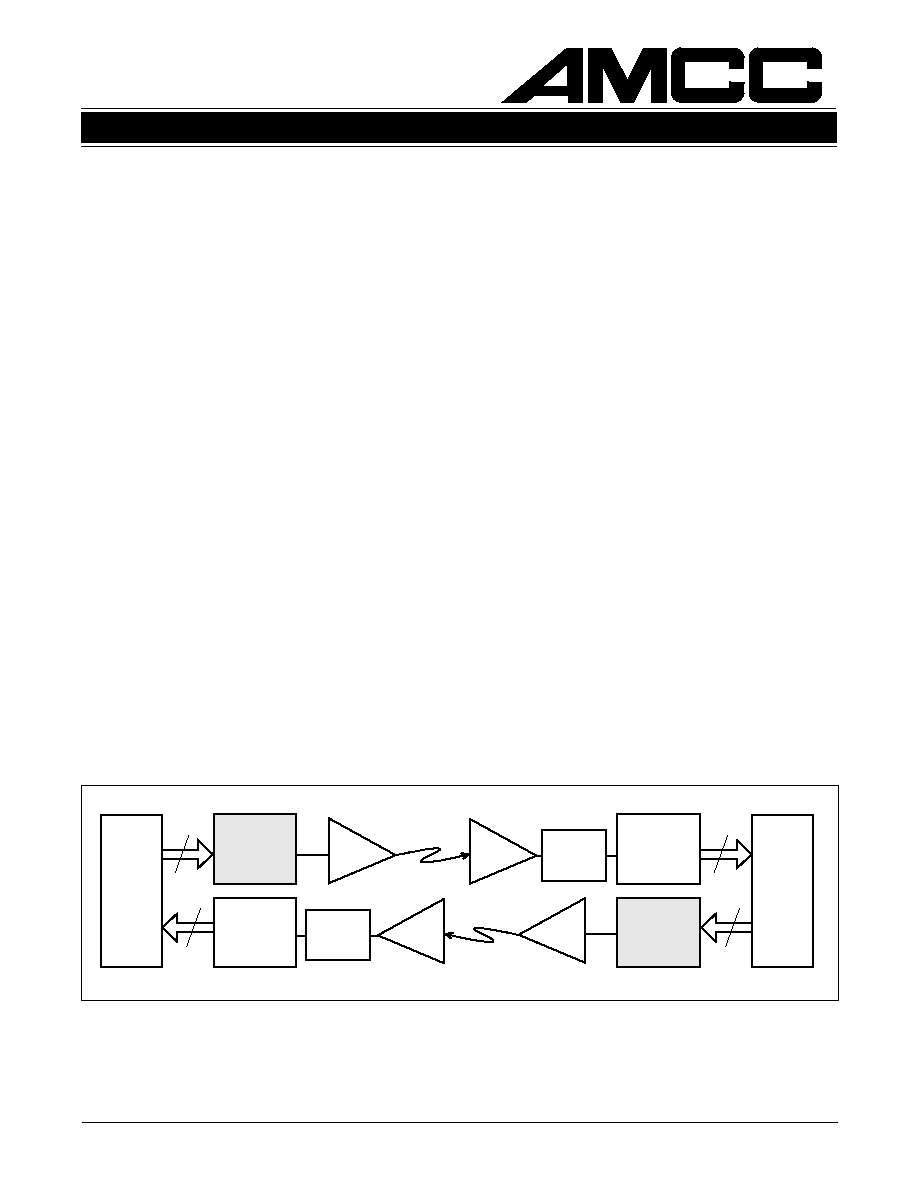
Figure 1. System Block Diagram
SONET/SDH/ATM OC-48 16:1 TRANSMITTER
S3083
GENERAL DESCRIPTION
The S3083 SONET/SDH MUX chip is a fully integrated
serialization SONET OC-48 (2.488 Gbps) interface de-
vice. The chip performs all necessary parallel-to-serial
functions in conformance with SONET/SDH transmis-
sion standards. The device is suitable for SONET-
based ATM applications. Figure 1 shows a typical
network application.
On-chip clock synthesis PLL components are con-
tained in the S3083 MUX chip allowing the use of a
slower external transmit clock reference. The chip
can be used with 155.52 MHz reference clock, in
support of existing system clocking schemes.
The low jitter LVPECL interface guarantees compli-
ance with the bit-error rate requirements of the
Bellcore and ITU-T standards. The S3083 is pack-
aged in a 80 PQFP/TEP, offering designers a small
package outline.
Network Interface
Processor
Network Interface
Processor
S3083
Tx
S3044
Rx
S3044
Rx
S3083
Tx
OTX
ORX
OTX
ORX
16
16
16
16
S3040
S3040

S3083
SONET/SDH/ATM OC-48 16:1 TRANSMITTER
2
August 27, 1999 / Revision B
SONET OVERVIEW
Synchronous Optical Network (SONET) is a standard
for connecting one fiber system to another at the opti-
cal level. SONET, together with the Synchronous
Digital Hierarchy (SDH) administered by the ITU-T,
forms a single international standard for fiber inter-
connect between telephone networks of different
countries. SONET is capable of accommodating a
variety of transmission rates and applications.
The SONET standard is a layered protocol with four
separate layers defined. These are:
∑ Photonic
∑ Section
∑ Line
∑ Path
Figure 2 shows the layers and their functions. Each
of the layers has overhead bandwidth dedicated to
administration and maintenance. The photonic layer
simply handles the conversion from electrical to optical
and back with no overhead. It is responsible for
transmitting the electrical signals in optical form over
the physical media. The section layer handles the
transport of the framed electrical signals across the
optical cable from one end to the next. Key functions
of this layer are framing, scrambling, and error moni-
toring. The line layer is responsible for the reliable
transmission of the path layer information stream
carrying voice, data, and video signals. Its main
functions are synchronization, multiplexing, and reli-
able transport. The path layer is responsible for the
actual transport of services at the appropriate signaling
rates.
Data Rates and Signal Hierarchy
Table 1 contains the data rates and signal designations
of the SONET hierarchy. The lowest level is the basic
SONET signal referred to as the synchronous transport
signal level-1 (STS-1). An STS-
N signal is made up of
N byte-interleaved STS-1 signals. The optical counter-
part of each STS-
N signal is an optical carrier level-N
signal (OC-
N). The S3083 chip supports the OC-48
data rate (2.488 Gbps).
Frame and Byte Boundary Detection
The SONET/SDH fundamental frame format for STS-48
consists of 144 transport overhead bytes followed by
Synchronous Payload Envelope (SPE) bytes. This
pattern of 144 overhead and 4176 SPE bytes is re-
peated nine times in each frame. Frame and byte
boundaries are detected using the A1 and A2 bytes
found in the transport overhead. (See Figure 3.)
For more details on SONET operations, refer to the
Bellcore SONET standard document.
Elec.
CCITT
Optical Data Rate (Mbps)
STS-1
OC-1
51.84
STS-3
STM-1
OC-3
155.52
STS-12
STM-4
OC-12
622.08
STS-24
STM-8
OC-24
1244.16
STS-48 STM-16
OC-48 2488.32
Table 1. SONET Signal Hierarchy
Figure 2. SONET Structure
Figure 3. STS-48/OC-48 Frame Format
9 Rows
48 A1
Bytes
48 A2
Bytes
A1 A1
A1 A1
A2 A2
A2 A2
Transport Overhead 144 Columns
144 x 9 = 1296 bytes
Synchronous Payload Envelope 4176 Columns
4176 x 9 = 37,584 bytes
125
µ
sec
s
s
End Equipment
Payload to
SPE mapping
Maintenance,
protection,
switching
Optical
transmission
Scrambling,
framing
Fiber Cable
End Equipment
Section layer
Photonic layer
Line layer
Path layer
Path layer
Section layer
Photonic layer
Line layer
Functions
3
S3083
SONET/SDH/ATM OC-48 16:1 TRANSMITTER
August 27, 1999 / Revision B
The sequence of operations is as follows:
Transmitter Operations:
1. 16-bit parallel input
2. Parallel-to-serial conversion
3. Serial output
Internal clocking and control functions are transpar-
ent to the user. Details of the data timing can be
seen in Figure 7, 18, and 19.
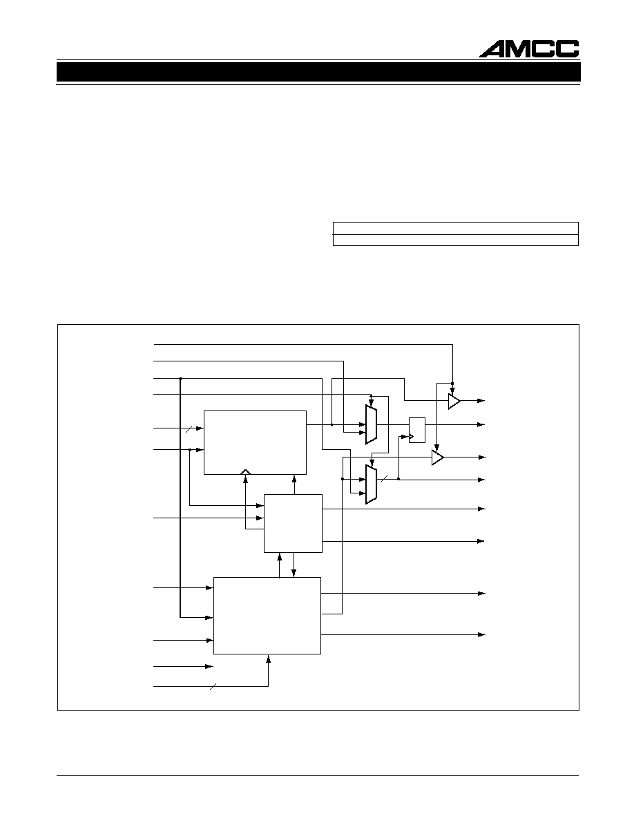
S3083 OVERVIEW
The S3083 transmitter implements SONET/SDH se-
rialization and transmission functions. The block dia-
gram in Figure 4 shows basic operation of the chip.
This chip can be used to implement the front end of
SONET equipment, which consists primarily of the
serial transmit interface and the serial receive inter-
face. The chip includes parallel-to-serial conversion
and system timing. The system timing circuitry con-
sists of a high-speed phase detector, clock dividers,
and clock distribution throughout the front end.
Figure 4. S3083 Functional Block Diagram
AMCC
S3040
OC-48 Clock Recovery Device
AMCC
S3044
OC-48 Receiver
Suggested Interface Devices
M
U
X
16
PIN[15:0]
LLDP/N
LLCLKP/N
LLEB
16:1 PARALLEL
TO SERIAL
TSDP/N
LSDP/N
DLEB
PICLKP/N
TIMING
GEN
PCLKP/N
TSCLKP/N
LOCKDET
155MCK
CLOCK
DIVIDER and
PHASE DETECTOR
RSTB
D
LSCLKP/N
2
TESTEN
REFCLKP/N
PHINIT
CAP1/2
2
PHERR
M
U
X

S3083
SONET/SDH/ATM OC-48 16:1 TRANSMITTER
4
August 27, 1999 / Revision B
S3083 ARCHITECTURE/FUNCTIONAL
DESIGN
MUX OPERATION
The S3083 performs the serializing stage in the pro-
cessing of a transmit SONET STS-48 bit serial data
stream. It converts the byte serial 155.52 Mbyte/sec
data stream to bit serial format at 2.488 Gbps. Diag-
nostic loopback is provided (transmitter to receiver),
and Line Loopback is also provided (receiver to trans-
mitter).
A high-frequency bit clock is generated from a
155.52 MHz frequency reference by using a fre-
quency synthesizer consisting of an on-chip phase-
locked loop circuit with a divider, VCO and loop filter.
Clock Divider and Phase Detector
The Clock Divider and Phase Detector, shown in the
block diagram in Figure 4, contains monolithic PLL
components that generate signals required to drive
the loop filter.
The REFCLK input must be generated from a differ-
ential LVPECL crystal oscillator which has a fre-
quency accuracy of better than the value stated in
Table 7 in order for the VCOCLK frequency to have
the same accuracy required for operation in a
SONET system.
In order to meet the 0.01 UI SONET jitter specifica-
tions, the maximum reference clock jitter must be
guaranteed over the 12 kHz to 20 MHz bandwidth.
For details of reference clock jitter requirements, see
Table 2.
The on≠chip phase detector, which compares the
phase relationship between the VCO input and the
REFCLK input, drives the loop filter.
Timing Generator
The Timing Generator function, seen in Figure 4, pro-
vides two separate functions. It provides a byte rate
version of the TSCLK, and a mechanism for aligning
the phase between the incoming byte clock and the
clock which loads the parallel-to-serial shift register.
The PCLK output is a byte rate version of TSCLK.
For STS-48, the PCLK frequency is 155.52 MHz.
PCLK is intended for use as a byte speed clock for
upstream multiplexing and overhead processing cir-
cuits. Using PCLK for upstream circuits will ensure a
stable frequency and phase relationship between the
data coming into and leaving the S3083 device.
In the parallel-to-serial conversion process, the in-
coming data is passed from the PICLK byte clock
timing domain to the internally generated byte clock
timing domain, which is phase aligned to the TSCLK.
The Timing Generator also produces a feedback ref-
erence clock to the Phase Detector. A counter divides
the synthesized clock down to the same frequency
as the reference clock REFCLK.
Parallel-to-Serial Converter
The Parallel-to-Serial converter shown in Figure 4 is
comprised of a FIFO and a parallel-to-serial register.
The FIFO input latches the data from the PIN[15:0]
bus on the rising edge of PICLK. The parallel-to-
serial register is a loadable shift register which takes
its parallel input from the FIFO output.
An internally generated divide by 16 clock, which is
phase aligned to the transmit serial clock as de-
scribed in the Timing Generator description, activates
the parallel data transfer between registers. The serial
data is shifted out of the parallel-to-serial register at
the TSCLK rate.
Table 2. Reference Jitter Limits
k
c
o
l
C
e
c
n
e
r
e
f
e
R
m
u
m
i
x
a
M
d
n
a
B
z
H
M
0
2
o
t
z
H
k
2
1
n
i
r
e
t
t
i
J
g
n
i
t
a
r
e
p
O
e
d
o
M
s
m
r
s
p
1
8
4
-
S
T
S

5
S3083
SONET/SDH/ATM OC-48 16:1 TRANSMITTER
August 27, 1999 / Revision B
FIFO
A FIFO is added to decouple the internal and exter-
nal (PICLK) clocks. The internally generated divide
by 16 clock is used to clock out data from the FIFO.
PHINIT and LOCKDET are used to center or reset
the FIFO. The PHINIT and LOCKDET signals will
center the FIFO after the third PICLK pulse. This is
in order to insure that PICLK is stable. This scheme
allows the user to have an infinite PCLK to PICLK
delay through the ASIC. Once the FIFO is initilized,
the PCLK to PICLK delay can have a maximum drift
as specified in Table 21.
FIFO Initialization
The FIFO can be initialized in one of the following
three ways:
1. During power up, once the PLL has locked to the
reference clock provided on the REFCLK pins,
the LOCKDET will go active and initialize the
FIFO.
2. When RSTB goes active, the entire chip is reset.
This causes the PLL to go out of lock and thus
the LOCKDET goes inactive. When the PLL reac-
quires the lock, the LOCKDET goes active and
initializes the FIFO. Note: PCLK is held reset
when RSTB is active.
3. The user can also initialize the FIFO by giving a
positive edge on PHINIT.
During the normal running operation, the incoming
data is passed from the PICLK timing domain to the
internally generated divide by 16 clock timing do-
main. Although the frequency of PICLK and the in-
ternally generated clock is the same, their phase
relationship is arbitrary. To prevent errors caused by
short setup or hold times between the two timing
domains, the timing generator circuitry monitors the
phase relationship between PICLK and the internally
generated clock. When a potential setup or hold time
violation is detected, the phase error goes High.
When PHERR conditions occur, PHINIT should be
activated to recenter the FIFO (at least 2 PCLK peri-
ods). This can be done by connecting PHERR to
PHINIT. When realignment occurs one to three bytes
of data will be lost. The user can also take in the
PHERR signal, process it and send an output to
PHINIT in such a way that idle bytes are lost during
the realignment process. PHERR will go inactive
when the realignment is complete. (See Figure 8.)
OTHER OPERATING MODES
Diagnostic Loopback
When the Diagnostic Loopback Enable (DLEB) input
is active, a loopback from the transmitter to the re-
ceiver at the serial data rate can be set up for diag-
nostic purposes. The differential serial output clock
and data from the transmitter (LSCLK and LSD) is
routed to the input of companion device in place of
the normal data stream (RSCLK and RSD).
Line Loopback
The Line Loopback circuitry consists of alternate
clock and data output drivers. For the S3083, it se-
lects the source of the data and clock which is output
on TSD and TSCLK. When the Line Loopback En-
able input (LLEB) is inactive, it selects data and
clock from the Parallel to Serial Converter block.
When LLEB is active, it forces the output data mul-
tiplexer to select data and clock from the LLD and
LLCLK inputs, and a receive-to-transmit loopback
can be established at the serial data rate.
TSCLK Powerdown
The user is advised not to connect pins 56, 57, 58
and 59 if TSCLKP/N output is not used. This should
be done to reduce the power and to get the best
results on the TSD output.