 | ÐлекÑÑоннÑй компоненÑ: FQV2105 | СкаÑаÑÑ:  PDF PDF  ZIP ZIP |
Microsoft Word - 285 3.3V - C.doc

FQV2105 · FQV295 · FQV285 · FQV275 · FQV265 · FQV255
OCTOBER 2002
FlexQ
TM
II
3F218C
© 2001 High Bandwidth Access, Inc. All rights reserved. Product specifications subject to change without notice.
Page 1 of 31
3.3 Volt Synchronous x18 First-In/First-Out Queue
Memory Configuration
Device
262,144 x 18
FQV2105
131,072 x 18
FQV295
65,536 x 18
FQV285
32,768 x 18
FQV275
16,384 x 18
FQV265
8,192 x 18
FQV255
Key Features
·
Industry leading First-In/First-Out Queues (up to 133MHz)
·
Write cycle time of 7.5ns independent of Read cycle time
·
Read cycle time of 7.5ns independent of Write cycle time
·
3.3V power supply
·
5V input tolerant on all control and data input pins
·
5V output tolerant on all flags and data output pins
·
Master Reset clears all previously programmed configurations including Write and Read pointers
·
Partial Reset clears Write and Read pointers but maintains all previously programmed configurations
·
First Word Fall Through (FWFT) and Standard Timing modes
·
Presets for eight different Almost Full and Almost Empty offset values
·
Parallel/Serial programming of PRAF and PRAE offset values
·
Full, Empty, Almost Full, Almost Empty, and Half Full indicators
·
Asynchronous output enable tri-state data output drivers
·
Data retransmission
·
Available package: 64 - pin Plastic Thin Quad Flat Pack (TQFP), 64 - pin Slim Thin Quad Flat Pack (STQFP)
·
(0°C to 70°C) Commercial operating temperature available for cycle time of 7.5ns and above
·
(-40°C to 85°C) Industrial operating temperature available for cycle time of 7.5ns and above
Product Description
HBA's FlexQTM II offers industry leading FIFO queuing bandwidth (up to 3.0 Gbps), with a wide range of memory
configurations (from 8,192 x 18 to 262,144 x 18). System designer has full flexibility of implementing deeper and wider queues
using FWFT mode and width expansion features. Full, Empty, and Half-Full indicators allow easy handshaking between
transmitters and receivers. User programmable Almost Full and Almost Empty (Parallel/Serial) indicators allow implementation
of virtual queue depths.
5V tolerant on all input and output pins allow easy interfacing with devices operating at higher voltage levels. Asynchronous
Output Enable pin configures the tri-state data output drivers. Independent Write and Read controls provide rate-matching
capability.
Master Reset clears all previously programmed configurations by providing a low pulse on MRST pin. In addition, Write and
Read pointers to the queue are initialized to zero. Partial Reset will not alter previously programmed configurations but will
initialize Write and Read pointers to zero.
In FWFT mode, first data written into the queue appears on output data bus after the specified latency period at the low to high
transition of RCLK. Subsequent reads from the queue will require asserting REN . This feature is useful when implementing
depth expansion functions. In this mode, DRDY and QRDY are used instead of FULL and EMPTY respectively.
In Standard mode, always assert REN for read operation. FULL and EMPTY are used instead of DRDY and
QRDY respectively.
PRAF
, PRAE , and HALF are available in either FWFT or Standard mode.
FQV2105 · FQV295 · FQV285 · FQV275 · FQV265 · FQV255
OCTOBER 2002
FlexQ
TM
II
3F218C
© 2001 High Bandwidth Access, Inc. All rights reserved. Product specifications subject to change without notice.
Page 2 of 31
Product Description (Continued)
At any time, data previously read from the queue can be retransmitted by asserting RET pin at the low to high transition of
RCLK for a retransmit operation. Retransmit initializes the Read pointer to zero. Hence, all re-reads will always start from the
physical 0
th
(Read pointer = zero) location of the queue. Both zero and normal latency timing modes are available for retransmit
operation.
These FlexQTM II devices have low power consumption, hence minimizing system power requirements. In addition, industry
standard 64 - pin Plastic TQFP and 64 - pin STQFP are offered to save system board space.
These queues are ideal for applications such as data communication, telecommunication, graphics, multiprocessing, test
equipment, network switching, etc.
FQV2105
FQV295
FQV285
FQV275
FQV265
FQV255
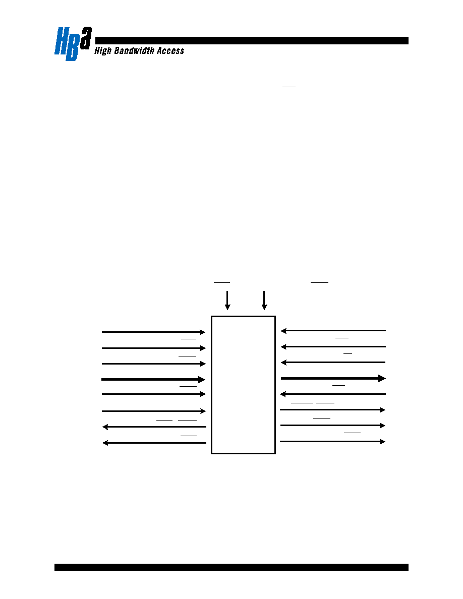
WRITE CLOCK (WCLK)
WRITE ENABLE ( )
LOAD ( )
x18 DATA IN (D
17 - 0
)
FIRST WORD FALL THROUGH/
SERIAL DATA INPUT (FWFT/SDI)
READ CLOCK (RCLK)
x18 DATA OUT (Q
17 - 0
)
PROGRAMMABLE ALMOST-
EMPTY ( )
HALF-FULL FLAG ( )
PARTIAL RESET ( )
MASTER RESET ( )
Block Diagram of Single Synchronous Queue
262,144 x 18 / 131,072 x 18 / 65,536 x 18 / 32,768 x 18 / 16,384 x 18 / 8,192 x 18
PRST
MRST
WEN
LOAD
PRAE
HALF
SERIAL DATA ENABLE ( )
SDEN
RETRANSMIT ( )
RET
OUTPUT ENABLE ( )
OE
READ ENABLE ( )
REN
EMPTY FLAG / OUTPUT READY
( / )
QRDY
EMPTY
FULL FLAG / INPUT READY
( / )
FULL DRDY
PROGRAMMABLE
ALMOST-FULL ( )
PRAF
Figure 1. Single Device Configuration Signal Flow Diagram
FQV2105 · FQV295 · FQV285 · FQV275 · FQV265 · FQV255
OCTOBER 2002
FlexQ
TM
II
3F218C
© 2001 High Bandwidth Access, Inc. All rights reserved. Product specifications subject to change without notice.
Page 3 of 31
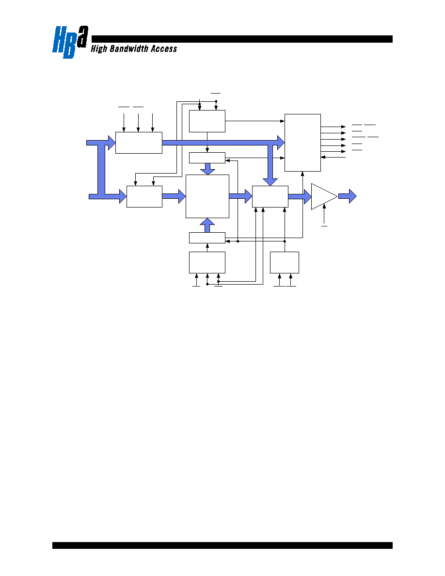
Offset Register
Write Control
Logic
Write Pointer
SRAM
Input Register
Output Register
Flag Logic
Output
Buffer
Q
17-0
x18
x18
D
17-0
Read Pointer
Read Control
Logic
Reset
FWFT/SDI
LOAD SDEN
WCLK
FWFT/SDI
PRAF
/
FULL
DRDY
PRAE
HALF
EMPTY QRDY
/
OE
MRST PRST
RCLK
RET
REN
WEN
Figure 2. Device Architecture
FQV2105 · FQV295 · FQV285 · FQV275 · FQV265 · FQV255
OCTOBER 2002
FlexQ
TM
II
3F218C
© 2001 High Bandwidth Access, Inc. All rights reserved. Product specifications subject to change without notice.
Page 4 of 31
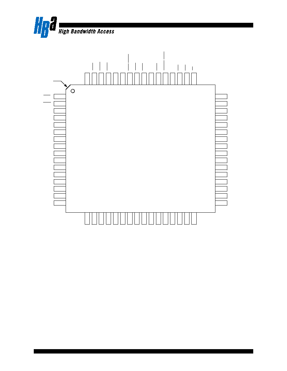
D
6
D
5
D
4
D
3
D
2
D
1
D
0
G
N
D
Q
0
Q
1
G
N
D
Q
2
Q
3
V
c
c
Q
4
Q
5
EM
P
T
Y/
QRDY
WC
LK
PR
ST
MR
ST
LOAD
FW
F
T
/
S
D
I
GND
FU
L
L
/
D
R
D
Y
PR
A
F
HALF
Vc
c
PR
A
E
RC
L
K
REN
RET
OE
Q17
Q16
GND
Q15
Q14
Vcc
Q13
Q12
Q11
GND
Q10
Q9
Q8
Q7
Q6
GND
WEN
SDEN
DC
(1)
Vcc
GND
D17
D16
D15
D14
D13
D12
D11
D10
D9
D8
D7
01
02
03
04
05
06
07
08
09
10
11
12
13
14
15
16
48
47
46
45
44
43
42
41
40
39
38
37
36
35
34
33
17
18
19
20
21
22
23
24
25
26
27
28
29
30
31
32
64
63
62
61
60
59
58
57
56
55
54
53
52
51
50
49
Index
TQFP - 64 (Drw No: PF-01A; Order code: PF)
STQFP - 64 (Drw No: TF-01A; Order code: TF)
Top View
NOTES:
1.
DC = Don't Care. Must be tied to GND or Vcc, cannot be left open.
Figure 3. Device Pin Out
FQV2105 · FQV295 · FQV285 · FQV275 · FQV265 · FQV255
OCTOBER 2002
FlexQ
TM
II
3F218C
© 2001 High Bandwidth Access, Inc. All rights reserved. Product specifications subject to change without notice.
Page 5 of 31
Pin #
Pin Name
Pin Symbol Input/Output
Description
62
Master Reset
MRST
Input
Master Reset is required to initialize Write and Read pointers to the
first position of the queue by setting MRST low. In Standard
mode, FULL and PRAF will go high; EMPTY and PRAE will go
low. In FWFT mode, DRDY will go low and QRDY will go high.
PRAF
and PRAE will go to the same state as Standard mode. In
both modes, all data outputs will go low. Previous programmed
configurations will not be maintained.
63 Partial
Reset
PRST
Input
Partial Reset is required to initialize Write and Read pointers to the
first position of the queue by setting PRST low. In Standard mode,
FULL
and PRAF will go high; EMPTY and PRAE will go low.
In FWFT mode, DRDY will go low and QRDY will go high.
PRAF
and PRAE will go to the same state as Standard mode. In
both modes, all data outputs will go low. Previous programmed
configurations will be maintained.
64 Write
Clock
WCLK Input
Writes data into queue during low to high transitions of WCLK if
WEN
is set to low.
1
Write Enable
WEN
Input
Controls write operation into queue or offset registers during low to
high transition of WCLK.
61 Load
Enable
LOAD
Input
During Master Reset, set LOAD low to select parallel
programming or one of eight default offset values. Set LOAD high
to select serial programming or one of eight default offset values.
After Master Reset, LOAD controls write/read, to/from offset
registers during low to high transition of WCLK/RCLK
respectively. Use in conjunction with WEN / REN .
6,7,8,9,
10,11,12,13,
14,15,16,17,
18,19,20,21,
22,23
Data Inputs
D
17 - 0
Input
18 - bit wide input data bus.
52 Read
Clock
RCLK Input
Reads data from queue during low to high transitions of RCLK if
REN
is set to low.
51 Read
Enable REN
Input
Controls read operation from queue or offset registers during low to
high transition of RCLK.
49 Output
Enable OE
Input
Setting OE low activates the data output drivers. Setting OE high
deactivates the data output drivers (High-Z).
48,47,45,44,
42,41,40,38,
37,36,35,34,
32,31,29,28,
26,25
Data Outputs
Q
17 - 0
Output
18 - bit wide output data bus.
60
First Word Fall
Through/Serial
Data Input
FWFT/SDI Input
Selects FWFT timing or Standard timing mode during Master
Reset. After Master Reset, if serial programming is selected
( LOAD = high), FWFT/SDI is used as the serial data input for the
offset registers. Serial data is written during the low to high
transition of WCLK. Use in conjunction with SDEN
.
Table 1. Pin Descriptions