 | –≠–ª–µ–∫—Ç—Ä–æ–Ω–Ω—ã–π –∫–æ–º–ø–æ–Ω–µ–Ω—Ç: RE024 | –°–∫–∞—á–∞—Ç—å:  PDF PDF  ZIP ZIP |

1
Features
∑
Dual Mode Low Drop Out Voltage Regulator
∑
2.8V Fixed Output Voltage
∑
3V to 5.5V Supply Operation
∑
160 mA Maximum Load Current in Full Power Mode
∑
Maximum Current Consumption 61 µA in Full Power Mode and 12 µA in Low Power Mode
∑
Power-down Mode Consumption Less Than 1 µA
∑
More Than 70dB (Typical) PSRR at 1 KHz
∑
70 µV
RMS
Output Noise
∑
0.35 µm CMOS Technology
∑
Typical Application: Baseband Memory Section Supply in Mobile Terminals
Description
RE024 is a dual mode Low Drop Out (LDO) voltage regulator macrocell with a fixed
2.8V output voltage, rated for loads up to 160 mA in full power mode and 5 mA in low
power mode. (Both modes can be selected by the LP2 signal.) It is designed to be
integrated with other analog cells, digital logic, microcontrollers, DSP cores and mem-
ory blocks into system-on-chip products.
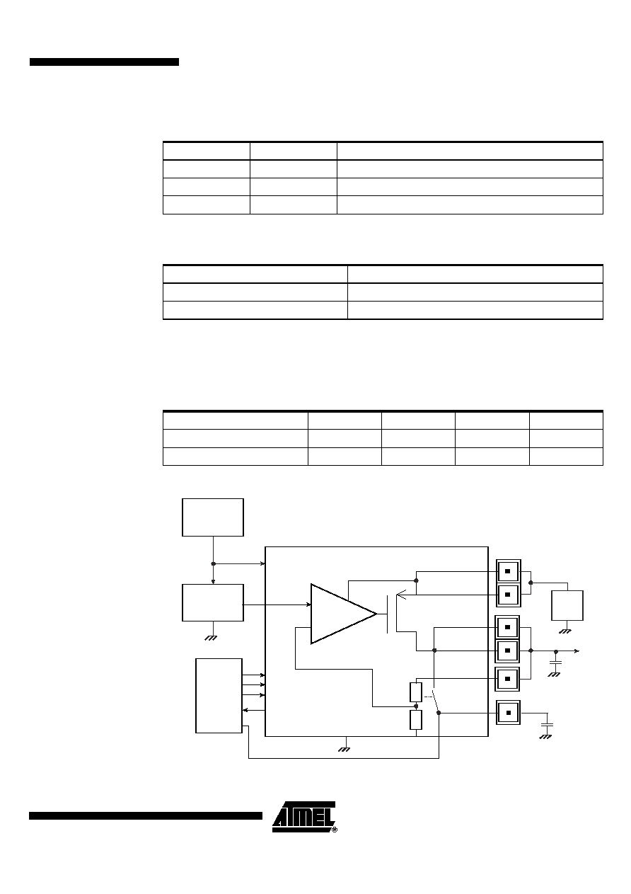
The circuit consists of a PMOS pass device, an error amplifier and a feedback resis-
tive network, sized to achieve the required closed loop gain. These blocks make up
the regulating loop. An over-current and short circuit protection circuit has been
included to limit the output current delivered by the regulator, thus avoiding destruction
in case of a short circuit.
An external reference voltage V
BG
(bandgap voltage) is necessary for correct function-
ality. The target reference voltage is 1.231V delivered, for example, by BG019. Double
pads on the supply voltage V
BAT2C
/V
BAT2CC
and output voltage V
MEMA
/V
MEMAA
are used
to reduce the total output resistance. Current reference is generated inside the cell
through a circuit supplied by a 2.5V ± 0.1V of regulated input voltage on V
SAUVC
.
Remote sense terminal V
MEMS
provides regulation of the load by connecting it to the
output terminal near a critical point to improve performance of the regulator (e.g., con-
necting it to the package pin by double-bonding, thus avoiding the bonding resistance
influence). A ceramic capacitor of 2.2 µF connected from V
MEMA
/V
MEMAA
to ground is
needed as external compensation.
A low-leakage current switch has been added to charge a second external capacitor
(2.2 µF - 10 µF) to V
MEMA
/V
MEMAA
. This voltage, called V
BACKUP
, is used to guarantee
30 minutes of operation time for the internal system clock and calendar in backup
mode when the main battery is unplugged.
Figure 1. Symbol
(1)
Note:
1. Pin names are written as they appear on the user screen when the symbol is
opened in the design tool environment.
V
SAUVC
GND2
V
BAT2C
V
BAT2CC
V
MEMA
V
MEMAA
V
BACKUP
V
BACKUPC
V
BG
ON2
LP2
BACKUPON
V
MEMC
V
MEMS
Embedded ASIC
Macrocell:
Power
Management for
Mobile
Terminals (PM)
RE024 2.8V
160 mA
Dual Mode LDO
Regulator
Rev. 2703B-PMGMT≠02/03

2
RE024 2.8V 160 mA Dual Mode LDO Regulator
2703B≠PMGMT≠02/03
Functional Diagram
Figure 2. Functional Diagram
Pin Description
Pin Name
I/O
Type
Function
Value
V
BAT2C
Power Supply
External Pad
Power Supply
3V to 5.5V
V
BAT2CC
Power Supply
External Pad
Power Supply
3V to 5.5V
V
MEMA
Analog Output
External Pad
Output Voltage
2.75V to 2.9
V
MEMAA
Analog Output
External Pad
Output Voltage
2.75V to 2.9V
V
MEMS
Analog Input
External Pad
Sense Voltage
2.75V to 2.9V
V
MEMC
Analog Output
Internal Pin
Output Voltage
2.75V to 2.9V
V
BACKUP
Analog Input
External Pad
Backup Voltage
2.75V to 2.9V
V
BACKUPC
Analog Output
Internal Pin
Internal Backup Voltage
2.75V to 2.9V
GND2
Analog Ground
Internal Pin
Ground
0
V
SAUVC
Positive Power Supply
Internal Pin
Power Supply
2.5V ± 0.1V
V
BG
Analog Input
Internal Pin
Voltage Reference
1.231V
ON2
Digital Input
Internal Pin
Enable Command
0V or V
BAT2C
/V
BAT2CC
LP2
Digital Input
Internal Pin
Low Power Mode Command
0V or V
BAT2C
/V
BAT2CC
BACKUPON
Digital Input
Internal Pin
Backup Mode Command
0V or V
BAT2C
/V
BAT2CC
V
MEMC
V
MEMA
V
MEMAA
V
BACKUP
V
BACKUPC
V
MEMS
V
BG
V
BG
V
BAT2C
V
BAT2CC
ON2
ON2
ON2
LP2
ON2
LP2
GND2
GND2
GND2
ON2
LP2
BACKUPON
R11
R21
R12
R22
IBIAS
ON2
SAUVC
Current Sensing
and Limiting
GND2
GND2
ON2, LP2
V

3
RE024 2.8V 160 mA Dual Mode LDO Regulator
2703B≠PMGMT≠02/03
Absolute Maximum Ratings
*
Electrical Specifications
(1)
T
J
= -20
∞
C to 125
∞
C, V
BAT2C
/V
BAT3CC
= 3V to 5.5V unless otherwise specified, output capacitance = 2.2 µF.
Analog Signals ....................................... -0.3V to 6.5V
*NOTICE:
Stresses beyond those listed under "Absolute Maxi-
mum Ratings" may cause permanent damage to the
device. This is a stress rating only and functional
operation of the device at these or other conditions
beyond those indicated in the operational sections of
this specification is not implied. Exposure to absolute
maximum rating conditions for extended periods may
affect device reliability.
Digital Signals......................................... -0.3V to 5.5V
Output Current................................... Internally limited
Junction Temperature ..........................-20
∞
C to 150
∞
C
Table 1. Electrical Characteristics
Symbol
Parameter
Condition
Min
Typ
Max
Unit
V
BAT2C
/V
BAT2CC
Operating Supply Voltage
3
5.5
V
V
SAUVC
Auxiliary Operating Supply
Voltage
2.4
2.5
2.6
V
T
J
Temperature Range
-20
125
∞C
Full Power Mode
V
MEMA
/V
MEMAA
Output Voltage
2.75
2.85
V
I
MEMA
/I
MEMAA
Output Current
160
mA
I
QQ
Quiescent Current
43
51
61
µA
V
DC
Line Regulation
I
MEMA
/I
MEMAA
= 160 mA
4
7
mV
V
TRAN
Transient Line Regulation
I
MEMA
/I
MEMAA
= 160 mA
rise time = fall time = 5 µs
18
33
mV
V
DC
Load Regulation
10% - 90% of max I
MEMA
/I
MEMAA
3
10
mV
V
TRAN
Transient Load Regulation
10% - 90% of max I
MEMA
/I
MEMAA
rise time = fall time = 5 µs
25
66
mV
PSRR
(2)
Power Supply Rejection Ratio
at Full Load
V
BAT2C
/
V
BAT2CC
= 3V
@100 Hz
-30
dB
@1 kHz
-30
dB
@20 kHz
-27
dB
@100 kHz
-20
dB
V
BAT2C
/
V
BAT2CC
=
4.25V
@100 Hz
-70
dB
@1 kHz
-70
dB
@20 kHz
-47
dB
@100 kHz
-32
dB
V
BAT2C
/
V
BAT2CC
= 5.5V
@100 Hz
-70
dB
@1 kHz
-65
dB
@20 kHz
-47
dB
@100 kHz
-30
dB
V
N
Output Noise
(3)
Bandwidth = 10 Hz to 100 kHz
70
118
µV
RMS
4
RE024 2.8V 160 mA Dual Mode LDO Regulator
2703B≠PMGMT≠02/03
Notes:
1. Obtained by considering the parasitics of a TFBGA100 Package.
2. This parameter shows the immunization of the circuit taking into account a voltage ripple on battery voltage for different fre-
quencies shown.
3. Obtained by using BG019 as reference voltage generator.
T
R
Rise Time
Full Load 10% - 90% of V
MEMA
/V
MEMAA
200
µs
I
SD
Shut Down Current
1
µA
I
CC
Short-circuit Current Threshold
450
mA
Low Power Mode
V
MEMA
/V
MEMAA
Output Voltage
2.72
2.9
V
I
MEMA
/I
MEMAA
Output Current
5
mA
I
QQ
Quiescent Current
9
10.5
12
µA
V
DC
Line Regulation
V
BAT2C
/V
BAT2CC
=
3.4V to 3.V
I
MEMA
/I
MEMAA
= 2 mA
2
3
mV
V
TRAN
Transient Line Regulation
V
BAT2C
/V
BAT2CC
= 3.4V to 3V
I
MEMA
/I
MEMAA
= 2 mA
rise time = fall time = 5 µs
2
4
mV
V
DC
Load Regulation
10% - 90% of max I
MEMA
/I
MEMAA
2
5
mV
V
TRAN
Transient Load Regulation
10% - 90% of max I
MEMA
/I
MEMAA
rise time = fall time = 5 µs
2
6
mV
PSRR
(2)
Power Supply Rejection Ratio
at Full Load
V
BAT2C
/
V
BAT2CC
= 3V
@100 Hz
-40
dB
@1 kHz
-40
dB
@20 kHz
-35
dB
@100 kHz
-35
dB
V
BAT2C
/
V
BAT2CC
=
4.25V
@100 Hz
-70
dB
@1 kHz
-65
dB
@20 kHz
-47
dB
@100 kHz
-30
dB
V
BAT2C
/
V
BAT2CC
= 5.5V
@100 Hz
-55
dB
@1 kHz
-55
dB
@20 kHz
-46
dB
@100 kHz
-35
dB
V
N
Output Noise
(3)
Bandwidth = 10 Hz to 100 kHz
204
300
µ V
RMS
T
R
Rise Time
Full Load 10% - 90% of V
MEMA
/V
MEMAA
500
µs
I
SD
Shut Down Current
1
µA
I
CC
Short-circuit Current Threshold
240
mA
Table 1. Electrical Characteristics (Continued)
Symbol
Parameter
Condition
Min
Typ
Max
Unit
5
RE024 2.8V 160 mA Dual Mode LDO Regulator
2703B≠PMGMT≠02/03
Control Modes
All digital signals are referred to the supply voltage V
BAT
.
Application
Example
A ceramic capacitor of 2.2 µF with ESR between 20 m
and 250 m
connected from
V
MEMA
/V
MEMAA
to ground is needed for external compensation.
A ceramic capacitor with a value between 2.2 µF and 10µF connected between V
BACKUP
and
Ground is used as backup supply.
Figure 3. Application Example
Table 2. Truth Table
ON2
LP2
V
MEMA
/V
MEMAA
0
X
Power down (High-Z)
1
0
Power on, Full Power Mode V
MEMA
/V
MEMAA
= 2.8V
1
1
Power on, Low Power Mode V
MEMA
/V
MEMAA
= 2.8V
Table 3. Backupon Truth Table
BACKUPON
V
BACKUP
0
Backup Mode
1
Backup Switch Closed V
BACKUP
= V
MEMA
/V
MEMAA
Description
Min
Typ
Max
Units
Capacitor (C
L
)
1.8
2.2
2.6
µF
Backup Battery (C
BCK
)
2.2
10
µF
Digital
Core
1.231V Bandgap
(e.g., BG019)
2.5V
2.5V Regulator
(e.g., RE031)
V
BAT2C
V
BAT2CC
V
MEMA
V
MEMAA
V
MEMS
V
BACKUP
V
BACKUPC
V
SAUVC
V
BG
ON6
LP2
BACKUPON
V
MEMC
Battery
Pack
GND2
C
L
C
BCK