KST-H017-000
1
STK830FC
Advanced Power MOSFET
S
S
e
e
m
m
i
i
c
c
o
o
n
n
d
d
u
u
c
c
t
t
o
o
r
r
Features
� Avalanche rugged technology.
� Low input capacitance.
� Improved gate charge.
� Low leakage current : 10uA (Max.) @ V
DS
=500V.
� Low R
DS(ON)
: 1.17(Typ.)
Ordering
Information
Type NO.
Marking
Package Code
STK830FC STK830 TO-220F-3SL
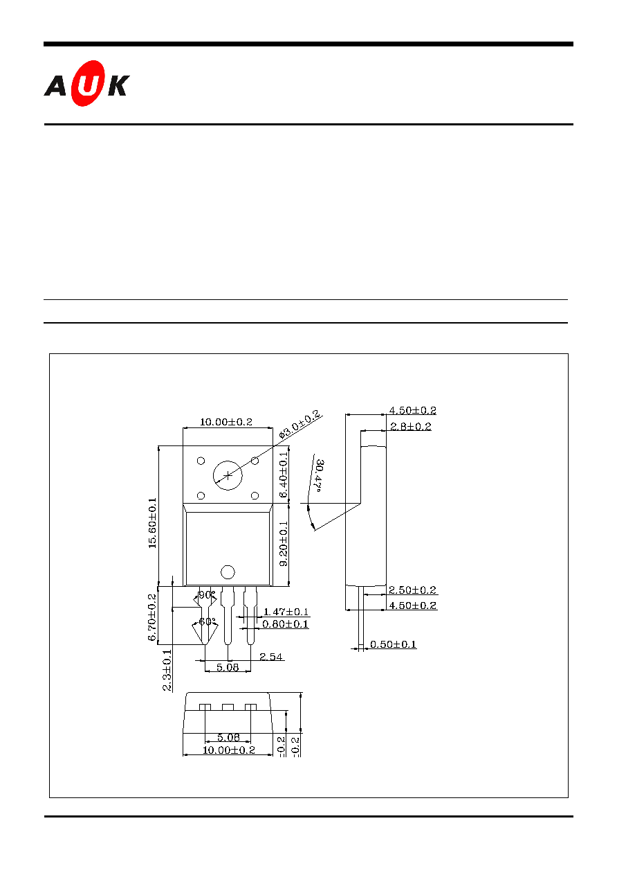
Outline Dimensions unit :
mm
PIN Connections
1. Gate
2. Drain
3. Source
KST-H017-000
2
STK830FC
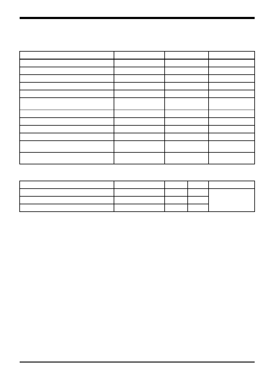
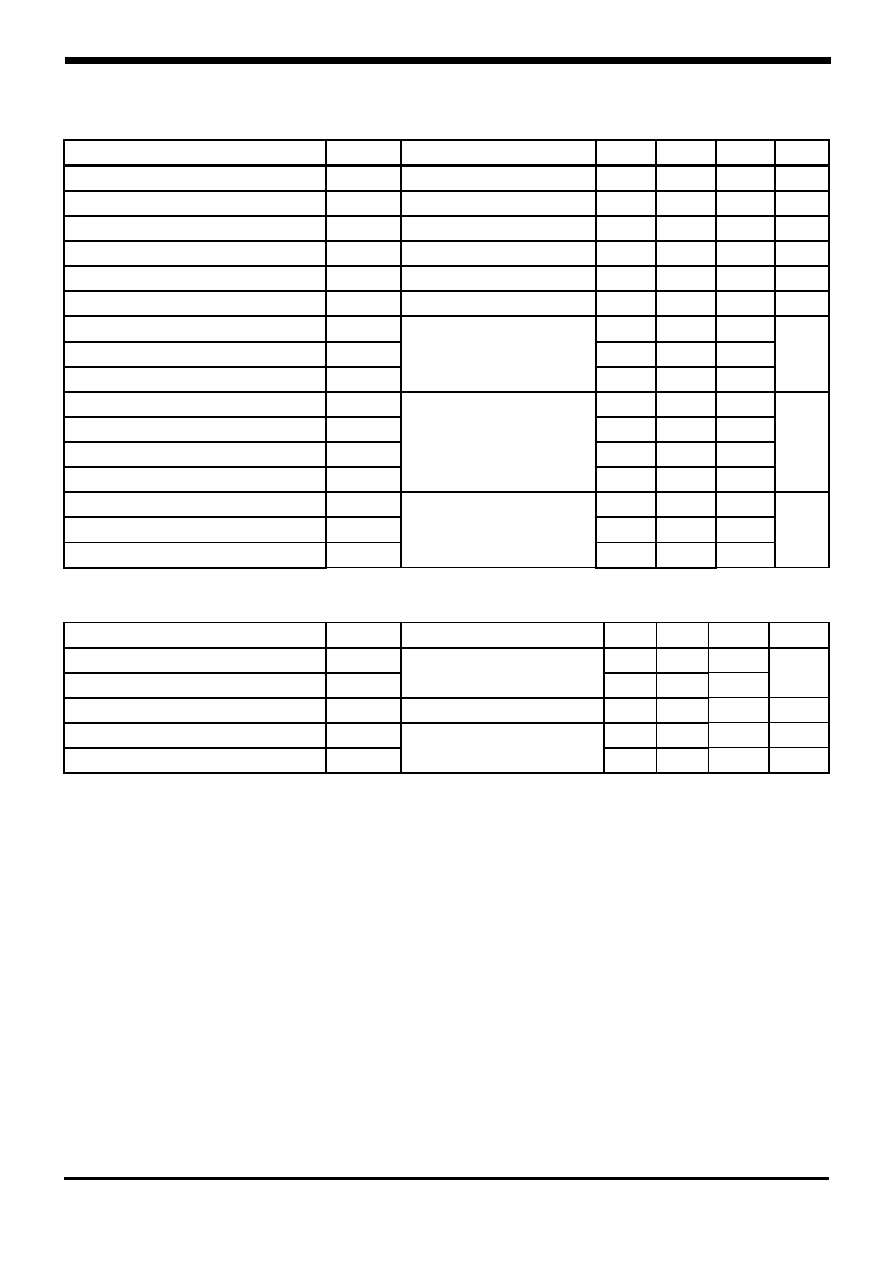
Absolute maximum ratings
Characteristic Symbol
Rating
Unit
Drain-Source voltage
V
DSS
500 V
Gate-Source voltage
V
GS
�30
V
Continuous Drain current (Tc=25)
I
D
4.5
*
A
Continuous Drain current (Tc=100)
I
D
2.9
*
A
Drain Current-Pulsed
I
DM
18 A
Power Dissipation (Tc=25)
Linear Derating Factor
P
D
38
0.3
W
W/
Single Pulsed Avalanche Energy
E
AS
270 mJ
Avalanche current
I
AR
4.5 A
Repetitive Avalanche Energy
E
AR
7.3 mJ
Peak Diode Recovery dv/dt
dv/dt
5.5
V/ns
Operating Junction and
Storage temperature range
T
J
, T
stg
-55~150 �C
Maximum lead temp. for soldering
Purpose, 1/8" from case for 5-seconds
T
L
300 �C
* Limited by Maximum junction Temperature
Thermal Resistance
Characteristic Symbol
Typ.
Max
Units
Junction-to-Case
R
JC
3.31
Case-to-Sink
R
CS
0.5
Junction-to-Ambient
R
JA
62.5
/W
KST-H017-000
3
STK830FC
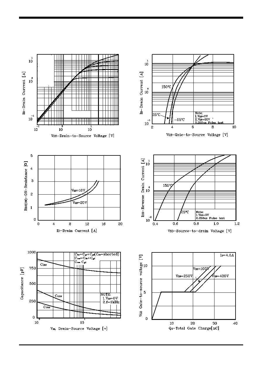
Electrical Characteristics
(Tc=25
�C unless otherwise specified)
Characteristic Symbol
Test
Condition
Min.
Typ.
Max.
Unit
Drain-Source breakdown voltage
BV
DSS
I
D
=250�A, V
GS
=0
500 V
Gate-Threshold voltage
V
GS(th)
I
D
=250�A, V
DS
=5V
2.0 4.0
V
Drain-source leakage current
I
DSS
V
DS
=500V
10
�A
Gate-source leakage
I
GSS
V
DS
=0V, V
GS
=�30V
�100
nA
Drain-Source on-resistance
R
DS(ON)
V
GS
=10V, I
D
=2.25A
1.5
Forward transconductance
g
fs
V
DS
=50V, I
D
=2.25A
3.87
S
Input capacitance
Ciss
760
900
Output capacitance
Coss
85
100
Reverse transfer capacitance
Crss
V
GS
=0V, V
DS
=25V, f=1MHz
15
22
pF
Turn-on delay time
t
d(on)
15
40
Rise time
t
r
16
40
Turn-off delay time
t
d(off)
66
140
Fall time
t
f
V
DD
=250V,I
D
=4.5A
R
G
=12
22
55
ns
Total gate charge
Q
g
33
43
Gate-source charge
Q
gs
4.4
Gate-drain("Miller")charge Q
gd
V
DS
=400V,V
GS
=10V,
I
D
=4.5A
16.6
nC
Source-Drain Diode Ratings and Characteristics
Characteristic Symbol
Test
Condition
Min
Typ
Max
Units
Continuous source current
I
S
4.5
Pulsed-source current
I
SM
Integral reverse pn-diode
in the MOSFET
18
A
Diode forward voltage
V
SD
T
J
=25, V
GS
=0V, I
S
=4.5A
1.4 V
Reverse recovery time
t
rr
285
ns
Reverse recovery charge
Q
rr
T
J
=25,I
F
=4.5A
di
F
/dt=100A/us
2.0
uC
Note ;
Repetitive Rating : Pulse Width Limited by Maximum Junction Temperature
L=30mH, I
AS
=4.5A, V
DD
=50V, R
G
=27 , starting T
J
=25
I
SD
4.5A, di/dt 130A/us, V
DD
BV
DSS
, starting T
J
=25
Pulse Test : Pulse Width=250us, Duty cycle 2%
Essentially independent of operating temperature