 | –≠–ї–µ–Ї—В—А–Њ–љ–љ—Л–є –Ї–Њ–Љ–њ–Њ–љ–µ–љ—В: CS5345 | –°–Ї–∞—З–∞—В—М:  PDF PDF  ZIP ZIP |

Advance Product Information
This document contains information for a new product.
Cirrus Logic reserves the right to modify this product without notice.
1
Copyright
©
Cirrus Logic, Inc. 2004
(All Rights Reserved)
Cirrus Logic, Inc.
www.cirrus.com
CS5345
105 dB, 24-Bit, 192 kHz Stereo Audio ADC
JUNE `04
DS658A1
A/D Features
Multi-bit Delta Sigma modulator
105 dB dynamic range
-95 dB THD+N
Stereo 6:1 Input Multiplexer
Programmable Gain Amplifier (PGA)
≠ +/- 12 dB gain, 0.5 dB step size
≠ Zero crossing, click-free transitions
Stereo microphone inputs
≠ +32 dB gain stage
≠ Low noise bias supply
Up to 192 kHz sampling rates
Selectable serial audio interface formats
≠ Left justified up to 24-bit
≠ I≤S up to 24-bit
High pass filter or DC offset calibration
System Features
Power down mode
+3.3 V to +5 V analog power supply, nominal
+3.3 V to +5 V digital power supply, nominal
Direct interface with 1.8 V to 5 V logic levels
Pin-compatible with CS4245
General Description
The CS5345 integrates an analog multiplexer, program-
mable gain amplifier, and stereo audio analog-to-digital
converter. The CS5345 performs stereo analog-to-digital
(A/D) conversion of up to 24-bit serial values at sample
rates up to 192 kHz.
A 6:1 stereo input multiplexer is included for selecting
between line level or microphone level inputs. The mi-
crophone input path includes a +32 dB gain stage and a
low noise bias voltage supply. The PGA is available for
line or microphone inputs and provides gain/attenuation
of
±12 dB in 0.5 dB steps.
The output of the PGA is followed by an advanced 5th-
order, multi-bit delta sigma modulator and digital filter-
ing/decimation. Sampled data is transmitted by the serial
audio interface at rates from 4 kHz to 192 kHz in either
slave or master mode.
Integrated level translators allow easy interfacing be-
tween the CS5345 and other devices operating over a
wide range of logic levels.
ORDERING INFORMATION
CS5345-CQZ -10∞ to 70∞ C
48-pin LQFP
CDB5345
Evaluation Board
1.8 V to 5 V
Line a r P hase
A nti-A lias F ilte r
Inte rna l V oltage
Re fe rence
Multibit
O versa mpling
A DC
Multibit
O ve rsa mpling
A D C
Line a r P hase
A nti-A lias F ilte r
H igh P a ss
F ilte r
H igh P a ss
F ilte r
S tere o Input 1
S e rial
A udio
O utput
3.3 V to 5 V
3.3 V to 5 V
MU X
P G A
PCM
Se
r
i
a
l
I
n
t
e
r
f
a
c
e
Re gister C onfigura tion
Le
v
e
l
T
r
an
s
l
at
o
r
Left P G A O utput
R ight P G A O utput
S tere o Input 2
S tere o Input 3
S tere o Input 4 /
Mic Input 1 & 2
S tere o Input 5
S tere o Input 6
P G A
+32 d B
+32 d B
L
e
ve
l
T
r
a
n
sl
a
t
o
r
Re se t
I≤C /S P I
C ontrol D ata
Inte rrupt
O ve rflow

CS5345
2
TABLE OF CONTENTS
1. PIN DESCRIPTIONS ............................................................................................................... 3
2. CHARACTERISTICS AND SPECIFICATIONS ....................................................................... 5
SPECIFIED OPERATING CONDITIONS ................................................................................. 5
ABSOLUTE MAXIMUM RATINGS ........................................................................................... 5
ADC ANALOG CHARACTERISTICS ....................................................................................... 6
ADC ANALOG CHARACTERISTICS ....................................................................................... 8
ADC DIGITAL FILTER CHARACTERISTICS ........................................................................... 9
PGAOUT ANALOG CHARACTERISTICS.............................................................................. 10
PGAOUT ANALOG CHARACTERISTICS (CONT'D)............................................................. 11
PGAOUT ANALOG CHARACTERISTICS (CONT'D)............................................................. 12
DC ELECTRICAL CHARACTERISTICS................................................................................. 13
DIGITAL INTERFACE CHARACTERISTICS.......................................................................... 14
SWITCHING CHARACTERISTICS - SERIAL AUDIO PORT ................................................. 15
SWITCHING CHARACTERISTICS - CONTROL PORT - I≤C FORMAT ................................ 18
SWITCHING CHARACTERISTICS - CONTROL PORT - SPI FORMAT ............................... 19
3. TYPICAL CONNECTION DIAGRAM ..................................................................................... 20
4. APPLICATIONS ..................................................................................................................... 21
4.1 Recommended Power-Up Sequence ............................................................................. 21
4.2 System Clocking ............................................................................................................. 21
4.2.1 Master Clock ...................................................................................................... 21
4.2.2 Master Mode ...................................................................................................... 22
4.2.3 Slave Mode ........................................................................................................ 22
4.3 High Pass Filter and DC Offset Calibration ..................................................................... 22
4.4 Analog Input Multiplexer, PGA, and Mic Gain ................................................................. 23
4.5 Input Connections ........................................................................................................... 23
4.6 PGA Auxiliary Analog Output .......................................................................................... 23
4.7 Control Port Description and Timing ............................................................................... 24
4.7.1 SPI Mode ........................................................................................................... 24
4.7.2 I≤C Mode ............................................................................................................ 25
4.8 Interrupts and Overflow ................................................................................................... 27
4.9 Reset ............................................................................................................................. 27
4.10 Synchronization of Multiple Devices ............................................................................. 27
4.11 Grounding and Power Supply Decoupling .................................................................... 27
5. REGISTER QUICK REFERENCE ......................................................................................... 28
6. REGISTER DESCRIPTION ................................................................................................... 29
6.1 Chip ID - Register 01h .................................................................................................... 29
6.2 Power Control - Address 02h .......................................................................................... 29
6.3 ADC Control - Address 04h ............................................................................................ 29
6.4 MCLK Frequency - Address 05h ..................................................................................... 30
6.5 PGAOut Control - Address 06h ....................................................................................... 31
6.6 Channel A PGA Control - Address 07h ........................................................................... 31
6.7 Channel B PGA Control - Address 08h ........................................................................... 31
6.8 ADC Input Control - Address 09h ................................................................................... 32
6.9 Active Level Control - Address 0Ch ................................................................................ 33
6.10 Interrupt Status - Address 0Dh ..................................................................................... 33
6.11 Interrupt Mask - Address 0Eh ....................................................................................... 34
6.12 Interrupt Mode MSB - Address 0Fh .............................................................................. 34
6.13 Interrupt Mode LSB - Address 10h ............................................................................... 34
7. PARAMETER DEFINITIONS ................................................................................................. 35
8. PACKAGE DIMENSIONS ...................................................................................................... 36
9. THERMAL CHARACTERISTICS AND SPECIFICATIONS ................................................. 36
Appendix A: Filter Plots ....................................................................................................... 37
CS5345
3
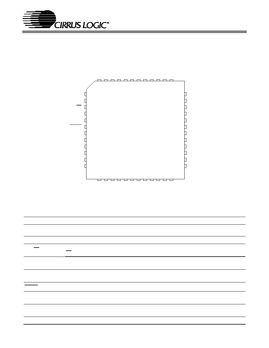
1. PIN DESCRIPTIONS
Pin Name
#
Pin Description
SDA/CDOUT
1
Serial Control Data (
Input
/
Output
) - SDA is a data I/O in I
2
C mode. CDOUT is the output data line for
the control port interface in SPI mode.
SCL/CCLK
2
Serial Control Port Clock (
Input
) - Serial clock for the serial control port.
AD0/CS
3
Address Bit 0 (I
2
C) / Control Port Chip Select (SPI)
(Input)
- AD0 is a chip address pin in I
2
C mode;
CS is the chip select signal for SPI format.
AD1/CDIN
4
Address Bit 1 (I
2
C) / Serial Control Data Input (SPI)
(Input)
- AD1 is a chip address pin in I
2
C mode;
CDIN is the input data line for the control port interface in SPI mode.
VLC
5
Control Port Power (
Input
) - Determines the required signal level for the control port interface. Refer
to the Recommended Operating Conditions for appropriate voltages.
RESET
6
Reset (
Input
) - The device enters a low power mode when this pin is driven low.
AIN3A
AIN3B
7,
8
Stereo Analog Input 3 (
Input
) - The full scale level is specified in the ADC Analog Characteristics
specification table.
AIN2A
AIN2B
9,
10
Stereo Analog Input 2 (
Input
) - The full scale level is specified in the ADC Analog Characteristics
specification table.
1
2
3
4
5
6
7
8
9
10
11
12
13 14 15 16 17 18 19 20 21 22 23 24
48 47 46 45 44 43 42 41 40 39 38 37
36
35
34
33
32
31
30
29
28
27
26
25
VLS
SDA/CDOUT
AG
N
D
OV
F
L
SCL/CCLK
AD0/CS
AD1/CDIN
VLC
RESET
AIN3A
AIN3B
AIN2A
AIN2B
AIN1A
AIN1B
VA
AF
I
L
T
B
VQ
TS
T
O
FI
L
T
+
TS
T
O
A
I
N4
A
/
M
I
CI
N1
A
I
N4
B
/
M
I
CI
N2
AIN
5
A
AIN
5
B
AF
I
L
T
A
TSTO
NC
NC
AGND
AGND
VA
PGAOUTB
PGAOUTA
AIN6B
AIN6A
MICBIAS
IN
T
VD
DGND
MC
LK
L
RCK
SC
L
K
SD
O
U
T
NC
NC
NC
TS
T
I
CS5345
CS5345
4
AIN1A
AIN1B
11,
12
Stereo Analog Input 1 (
Input
) - The full scale level is specified in the ADC Analog Characteristics
specification table.
AGND
13
Analog Ground (
Input
) - Ground reference for the internal analog section.
VA
14
Analog Power
(Input)
- Positive power for the internal analog section.
AFILTA
15
Antialias Filter Connection (
Output
) - Antialias filter connection for the channel A ADC input.
AFILTB
16
Antialias Filter Connection (
Output
) - Antialias filter connection for the channel B ADC input.
VQ
17
Quiescent Voltage (
Output
) - Filter connection for the internal quiescent reference voltage.
TSTO
18
Test Pin (
Output
) - This pin must be left unconnected.
FILT+
19
Positive Voltage Reference (
Output
) - Positive reference voltage for the internal sampling circuits.
TSTO
20
Test Pin - This pin must be left unconnected.
AIN4A/MICIN1
AIN4B/MICIN2
21,
22
Stereo Analog Input 4 / Microphone Input 1 & 2 (
Input
) - The full scale level is specified in the ADC
Analog Characteristics specification table.
AIN5A
AIN5B
23,
24
Stereo Analog Input 5 (
Input
) - The full scale level is specified in the ADC Analog Characteristics
specification table.
MICBIAS
25
Microphone Bias Supply (
Output
) - Low noise bias supply for external microphone. Electrical charac-
teristics are specified in the DC Electrical Characteristics specification table.
AIN6A
AIN6B
26,
27
Stereo Analog Input 6 (
Input
) - The full scale level is specified in the ADC Analog Characteristics
specification table.
PGAOUTA
PGAOUTB
28,
29
PGA Analog Audio Output (
Output
) - Either an analog output from the PGA block or high impedance.
See "PGAOut Source Select (Bit 6)" on page 31.
VA
30
Analog Power
(Input)
- Positive power for the internal analog section.
AGND
31,
32
Analog Ground (
Input
) - Ground reference for the internal analog section.
NC
33,
34
No Connect - These pins are not connected internally and should be tied to ground to minimize any
potential coupling effects.
TSTO
35
Test Pin (
Output
) - This pin must be left unconnected.
VLS
36
Serial Audio Interface Power (
Input
) - Determines the required signal level for the serial audio inter-
face. Refer to the Recommended Operating Conditions for appropriate voltages.
TSTI
37
Test Pin (
Input
) - This pin must be connected to ground.
NC
38,
39,
40
No Connect - These pins are not connected internally and should be tied to ground to minimize any
potential coupling effects.
SDOUT
41
Serial Audio Data Output (
Output
) - Output for two's complement serial audio data.
SCLK
42
Serial Clock
(Input/Output
) - Serial clock for the serial audio interface.
LRCK
43
Left Right Clock
(Input/Output
) - Determines which channel, Left or Right, is currently active on the
serial audio data line.
MCLK
44
Master Clock (
Input/Output
) -Clock source for the ADC's delta-sigma modulators.
DGND
45
Digital Ground (
Input
) - Ground reference for the internal digital section.
VD
46
Digital Power (
Input
) - Positive power for the internal digital section.
INT
47
Interrupt (
Output
) - Indicates an interrupt condition has occurred.
OVFL
48
Overflow (
Output
) - Indicates an ADC overflow condition is present.
CS5345
5
2. CHARACTERISTICS AND SPECIFICATIONS
(All Min/Max characteristics and specifications are guaranteed over the Specified Operating Conditions. Typical
performance characteristics and specifications are derived from measurements taken at nominal supply voltages
and T
A
= 25
∞C.)
SPECIFIED OPERATING CONDITIONS
(AGND = DGND = 0 V; All voltages with respect to
ground.)
ABSOLUTE MAXIMUM RATINGS
(AGND = DGND = 0 V All voltages with respect to ground.) (Note
1)
Notes: 1. Operation beyond these limits may result in permanent damage to the device.
Normal operation is not guaranteed at these extremes.
2. Any pin except supplies. Transient currents of up to ±100 mA on the analog input pins will not cause
SCR latch-up.
Parameters
Symbol Min Nom
Max
Units
DC Power Supplies:
Analog
Digital
Logic - Serial Port
Logic - Control Port
VA
VD
VLS
VLC
3.1
3.1
1.71
1.71
5.0
3.3
3.3
3.3
5.25
5.25
5.25
5.25
V
V
V
V
Ambient Operating Temperature (Power Applied)
T
A
-10
-
+70
∞C
Parameter
Symbol
Min
Typ
Max
Units
DC Power Supplies:
Analog
Digital
Logic - Serial Port
Logic - Control Port
VA
VD
VLS
VLC
-0.3
-0.3
-0.3
-0.3
-
-
-
-
+6.0
+6.0
+6.0
+6.0
V
V
V
V
Input Current
(Note 2)
I
in
-
-
±10
mA
Analog Input Voltage
V
INA
AGND-0.3
-
VA+0.3
V
Digital Input Voltage
Logic - Serial Port
Logic - Control Port
V
IND-S
V
IND-C
-0.3
-0.3
-
-
VLS+0.3
VLC+0.3
V
V
Ambient Operating Temperature (Power Applied)
T
A
-20
-
+85
∞C
Storage Temperature
T
stg
-65
-
+150
∞C