 | –≠–ª–µ–∫—Ç—Ä–æ–Ω–Ω—ã–π –∫–æ–º–ø–æ–Ω–µ–Ω—Ç: CS5381-KZ | –°–∫–∞—á–∞—Ç—å:  PDF PDF  ZIP ZIP |
Advance Product Information
This document contains information for a new product.
Cirrus Logic reserves the right to modify this product without notice.
1
Copyright
© Cirrus Logic, Inc. 2002
(All Rights Reserved)
Cirrus Logic, Inc.
http://www.cirrus.com
CS5381
120 dB, 192 kHz, Multi-Bit Audio A/D Converter
Features
Advanced Multi-bit Delta-Sigma Architecture
24-Bit Conversion
120 dB Dynamic Range
-105 dB THD+N
Supports all Audio Sample Rates Including
192 kHz
Less than 325 mW Power Consumption
High Pass Filter or DC Offset Calibration
Supports Logic Levels Between 5 and 2.5V
Differential Analog Architecture
Linear Phase Digital Anti-Alias Filtering
Overflow Detection
Pin compatible with the CS5361
General Description
The CS5381 is a complete analog-to-digital converter for
digital audio systems. It performs sampling, analog-to-
digital conversion and anti-alias filtering, generating
24-bit values for both left and right inputs in serial form at
sample rates up to 200kHz per channel.
The CS5381 uses a 5th-order, multi-bit delta-sigma
modulator followed by digital filtering and decimation,
which removes the need for an external anti-alias filter.
The ADC uses a differential architecture which provides
excellent noise rejection.
The CS5381 is ideal for audio systems requiring wide dy-
namic range, negligible distortion and low noise, such as
A/V receivers, DVD-R, CD-R, digital mixing consoles,
and effects processors.
ORDERING INFORMATION
CS5381-KS
-10∞ to 70∞ C
24-pin SOIC
CS5381-KZ
-10∞ to 70∞ C
24-pin TSSOP
CDB5381
Evaluation Board
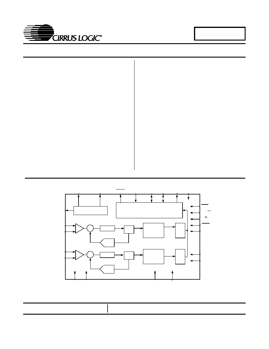
Voltage Reference
Serial Output Interface
Digital
Filter
High
Pass
Filter
High
Pass
Filter
Decimation
Digital
Filter
Decimation
DAC
-
+
S/H
DAC
-
+
S/H
AINR+
SCLK
SDOUT MCLK
RST
VQ
LRCK
AINR-
AINL+
AINL-
FILT+
I
2
S/LJ
M/S
HPF
MODE0
MODE1
REFGND
V
L
MDIV
LP Filter
LP Filter
OVFL
GND
VA
5.0V
GND
VD
3.3V - 5.0V
2.5V - 5.0V
DEC `02
DS563A1

CS5381
2
TABLE OF CONTENTS
1 PIN DESCRIPTIONS ................................................................................................................. 4
2 CHARACTERISTICS AND SPECIFICATIONS ......................................................................... 5
SPECIFIED OPERATING CONDITIONS ................................................................................. 5
ABSOLUTE MAXIMUM RATINGS ........................................................................................... 5
ANALOG CHARACTERISTICS (CS5381-KS/KZ) .................................................................... 6
DIGITAL FILTER CHARACTERISTICS.................................................................................... 7
SWITCHING CHARACTERISTICS - SERIAL AUDIO PORT ................................................... 8
DC ELECTRICAL CHARACTERISTICS................................................................................. 11
DIGITAL CHARACTERISTICS ............................................................................................... 11
3 TYPICAL CONNECTION DIAGRAM ....................................................................................... 12
4 APPLICATIONS ....................................................................................................................... 13
4.1 Operational Mode/Sample Rate Range Select ................................................................ 13
4.2 System Clocking .............................................................................................................. 13
4.2.1 Master Mode ....................................................................................................... 13
4.2.2 Slave Mode ......................................................................................................... 14
4.3 Power-up Sequence ........................................................................................................ 14
4.4 Analog Connections ......................................................................................................... 14
4.5 High Pass Filter and DC Offset Calibration ..................................................................... 15
4.6 Overflow Detection ........................................................................................................... 16
4.6.1 OVFL Output Timing ........................................................................................... 16
4.7 Grounding and Power Supply Decoupling ....................................................................... 16
4.8 Synchronization of Multiple Devices ................................................................................ 16
5 PACKAGE DIMENSIONS......................................................................................................... 17
THERMAL CHARACTERISTICS............................................................................................ 18
6 PARAMETER DEFINITIONS ................................................................................................... 19
7 APPENDIX ............................................................................................................................... 20
Contacting Cirrus Logic Support
For all product questions and inquiries contact a Cirrus Logic Sales Representative.
To find one nearest you go to
http://www.cirrus.com/corporate/contacts/sales.cfm
IMPORTANT NOTICE
"Preliminary" product information describes products that are in production, but for which full characterization data is not yet available. "Advance" product infor-
mation describes products that are in development and subject to development changes. Cirrus Logic, Inc. and its subsidiaries ("Cirrus") believe that the infor-
mation contained in this document is accurate and reliable. However, the information is subject to change without notice and is provided "AS IS" without warranty
of any kind (express or implied). Customers are advised to obtain the latest version of relevant information to verify, before placing orders, that information being
relied on is current and complete. All products are sold subject to the terms and conditions of sale supplied at the time of order acknowledgment, including those
pertaining to warranty, patent infringement, and limitation of liability. No responsibility is assumed by Cirrus for the use of this information, including use of this
information as the basis for manufacture or sale of any items, or for infringement of patents or other rights of third parties. This document is the property of Cirrus
and by furnishing this information, Cirrus grants no license, express or implied under any patents, mask work rights, copyrights, trademarks, trade secrets or
other intellectual property rights. Cirrus owns the copyrights of the information contained herein and gives consent for copies to be made of the information only
for use within your organization with respect to Cirrus integrated circuits or other parts of Cirrus. This consent does not extend to other copying such as copying
for general distribution, advertising or promotional purposes, or for creating any work for resale.
An export permit needs to be obtained from the competent authorities of the Japanese Government if any of the products or technologies described in this ma-
terial and controlled under the "Foreign Exchange and Foreign Trade Law" is to be exported or taken out of Japan. An export license and/or quota needs to be
obtained from the competent authorities of the Chinese Government if any of the products or technologies described in this material is subject to the PRC Foreign
Trade Law and is to be exported or taken out of the PRC.
CERTAIN APPLICATIONS USING SEMICONDUCTOR PRODUCTS MAY INVOLVE POTENTIAL RISKS OF DEATH, PERSONAL INJURY, OR SEVERE
PROPERTY OR ENVIRONMENTAL DAMAGE ("CRITICAL APPLICATIONS"). CIRRUS PRODUCTS ARE NOT DESIGNED, AUTHORIZED, OR WARRANT-
ED TO BE SUITABLE FOR USE IN LIFE-SUPPORT DEVICES OR SYSTEMS OR OTHER CRITICAL APPLICATIONS. INCLUSION OF CIRRUS PRODUCTS
IN SUCH APPLICATIONS IS UNDERSTOOD TO BE FULLY AT THE CUSTOMER'S RISK.
Cirrus Logic, Cirrus, and the Cirrus Logic logo designs are trademarks of Cirrus Logic, Inc. All other brand and product names in this document may be trade-
marks or service marks of their respective owners.

CS5381
3
LIST OF FIGURES
Figure 1. Master Mode, Left Justified SAI ....................................................................................... 9
Figure 2. Slave Mode, Left Justified SAI ......................................................................................... 9
Figure 3. Master Mode, I
2
S SAI ...................................................................................................... 9
Figure 4. Slave Mode, I
2
S SAI ........................................................................................................ 9
Figure 5. OVFL Output Timing ........................................................................................................ 9
Figure 6. Left Justified Serial Audio Interface ............................................................................... 10
Figure 7. I
2
S Serial Audio Interface............................................................................................... 10
Figure 8. OVFL Output Timing, I2S Format .................................................................................. 10
Figure 9. OVFL Output Timing, Left-Justified Format ................................................................... 10
Figure 10. Typical Connection Diagram ........................................................................................ 12
Figure 11. CS5381 Master Mode Clocking ................................................................................... 13
Figure 12. Recommended Analog Input Buffer............................................................................. 15
Figure 13. Single Speed Mode Stopband Rejection ..................................................................... 20
Figure 14. Single Speed Mode Transition Band ........................................................................... 20
Figure 15. Single Speed Mode Transition Band (Detail)............................................................... 20
Figure 16. Single Speed Mode Passband Ripple ......................................................................... 20
Figure 17. Double Speed Mode Stopband Rejection.................................................................... 20
Figure 18. Double Speed Mode Transition Band .......................................................................... 20
Figure 19. Double Speed Mode Transition Band (Detail) ............................................................. 21
Figure 20. Double Speed Mode Passband Ripple ........................................................................ 21
Figure 21. Quad Speed Mode Stopband Rejection ...................................................................... 21
Figure 22. Quad Speed Mode Transition Band............................................................................. 21
Figure 23. Quad Speed Mode Transition Band (Detail) ................................................................ 21
Figure 24. Quad Speed Mode Passband Ripple........................................................................... 21
LIST OF TABLES
Table 1. CS5381 Mode Control..................................................................................................... 13
Table 2. CS5381 Common Master Clock Frequencies................................................................. 14
Table 3. CS5381 Slave Mode Clock Ratios .................................................................................. 14

CS5381
4
1
PIN DESCRIPTIONS
Power Supply and Ground
Pin Name
#
Pin Description
RST
1
Reset (Input) - The device enters a low power mode when low.
M/S
2
Master/Slave Mode (Input) - Selects operation as either clock master or slave.
LRCK
3
Left Right Clock (Input/Output) - Determines which channel, Left or Right, is currently active on the
serial audio data line.
SCLK
4
Serial Clock (Input/Output) - Serial clock for the serial audio interface.
MCLK
5
Master Clock (Input) - Clock source for the delta-sigma modulator and digital filters.
VD
6
Digital Power (Input) - Positive power supply for the digital section.
GND
7,18
Ground (Input) - Ground reference. Must be connected to analog ground.
VL
8
Logic Power (Input) - Positive power for the digital input/output.
SDOUT
9
Serial Audio Data Output (Output) - Output for two's complement serial audio data.
MDIV
10
MCLK Divider (Input) - Enables a master clock divide by two function.
HPF
11
High Pass Filter Enable (Input) - Enables the Digital High-Pass Filter.
I
2
S/LJ
12
Serial Audio Interface Format Select (Input) -Selects either the left-justified or I
2
S format for the SAI.
M0
M1
13,
14
Mode Selection (Input) - Determines the operational mode of the device.
OVFL
15
Overflow (Output, open drain) - Detects an overflow condition on both left and right channels.
AINL+
AINL-
16,
17
Differential Left Channel Analog Input (Input) - Signals are presented differentially to the delta-sigma
modulators via the AINL+/- pins.
VA
19
Analog Power (Input) - Positive power supply for the analog section.
AINR+
AINR-
20,
21
Differential Right Channel Analog Input (Input) -Signals are presented differentially to the delta-sigma
modulators via the AINR+/- pins.
VQ
22
Quiescent Voltage (Output) - Filter connection for the internal quiescent reference voltage.
REF_GND
23
Reference Ground (Input) - Ground reference for the internal sampling circuits.
FILT+
24
Positive Voltage Reference (Output) - Positive reference voltage for the internal sampling circuits.
RST
1
24
FILT+
M/S
2
23
REFGND
LRCK
3
22
VQ
SCLK
4
21
AINR+
MCLK
5
20
AINR-
VD
6
19
VA
GND
7
18
GND
VL
8
17
AINL-
SDOUT
9
16
AINL+
MDIV
10
15
OVFL
HPF
11
14
M1
I
2
S/LJ
12
13
M0

CS5381
5
2 CHARACTERISTICS AND SPECIFICATIONS
(All Min/Max characteristics and specifications are guaranteed over the Specified operating Conditions. Typical per-
formance characteristics and specifications are derived from measurements taken at VA = 5.0V, VD = VL = 3.3V,
and TA = 25 C.)
SPECIFIED OPERATING CONDITIONS
(GND = 0 V; all voltages with respect to 0 V.)
ABSOLUTE MAXIMUM RATINGS
(GND = 0V, All voltages with respect to ground.) (Note 3)
Notes: 1. Any pin except supplies. Transient currents of up to ±100 mA on the analog input pins will not cause SRC
latch-up.
2. The maximum over/under voltage is limited by the input current.
3. Operation beyond these limits may result in permanent damage to the device. Normal operation is not
guaranteed at these extremes.
Parameters
Symbol
Min
NOM
Max
Units
DC Power Supply
DC Power Supplies:
Positive Analog
Positive Digital
Positive Logic
VA
VD
VL
4.75
3.1
2.37
5.0
-
-
5.25
5.25
5.25
V
V
V
Ambient Operating Temperature (Power Applied)
T
A
-10
-
+70
∞C
Parameter
Symbol
Min
Typ
Max
Units
DC Power Supplies:
Analog
Logic
Digital
VA
VL
VD
-0.3
-0.3
-0.3
-
-
-
+6.0
+6.0
+6.0
V
V
V
Input Current
(Note 1)
I
in
-
-
±10
mA
Analog Input Voltage
(Note 2)
V
IN
GND-0.7
-
VA+0.7
V
Digital Input Voltage
(Note 2)
V
IND
-0.7
-
VL+0.7
V
Ambient Operating Temperature (Power Applied)
T
A
-50
-
+95
∞C
Storage Temperature
T
stg
-65
-
+150
∞C