Spread AwareTM, Two-output Zero Delay Buffer
CY2502
Cypress Semiconductor Corporation
∑
3901 North First Street
∑
San Jose
∑
CA 95134
∑
408-943-2600
Document #: 38-07277 Rev. *B
Revised December 21, 2002
2
Features
∑ Spread AwareTM designed to work with SSFT reference
signals
∑ Well-suited to both 33- and 66-MHz designs
∑ 3.3V power supply
∑ On-chip 25
damping resistors
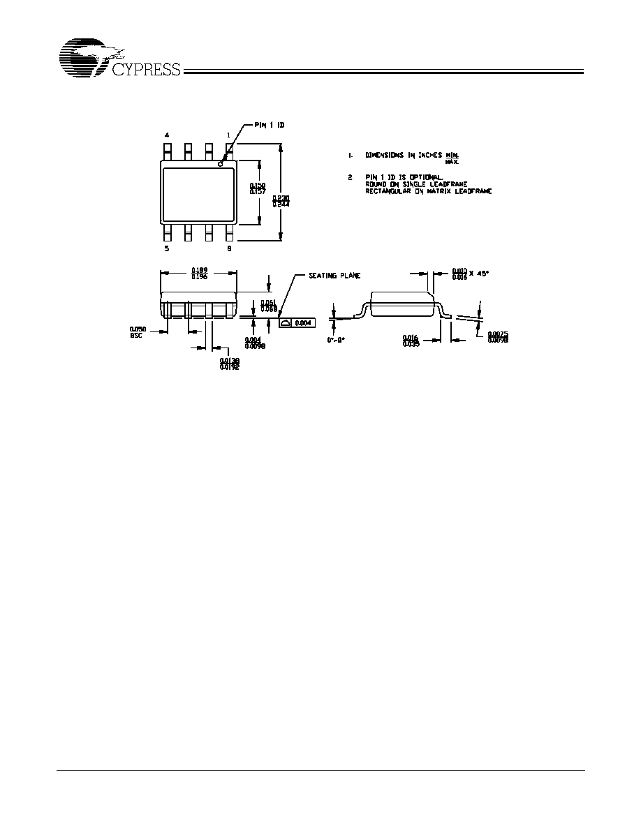
∑ Available in 8-pin SOIC package
Key Specifications
Operating Voltage:............................................... 3.3V ± 10%
Operating Range: ............................. 25 MHz < f
out
< 85 MHz
Cycle-to-cycle Jitter: .................................................< 150 ps
Phase Error Jitter .....................................................< 150 ps
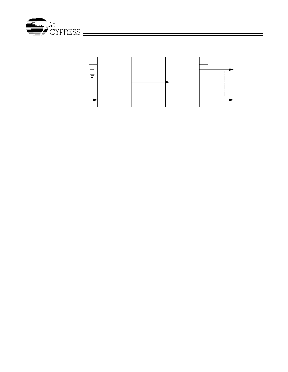
Block Diagram
Pin Configuration
8 pin SOIC
1
2
3
4
8
7
6
5
CLKIN
AVDD
GND
FBIN
AGND
FBOUT
CLKOUT
VDD
Schematic
1
2
3
4
8
7
6
5
CLKIN
AVDD
GND
FBIN
AGND
FBOUT
CLKOUT
VDD
FB
3.3V
.1uF
10uF
FB
3.3V
.1uF
10uF
PLL
CLKOUT
FBOUT
CLKIN
FBIN
CY2502
Document #: 38-07277 Rev. *B
Page 2 of 6
Overview
The integrated PLL of the CY2502 provides two low-jitter,
low-skew clock outputs. One of these outputs, FBOUT, is used
as feedback to the PLL, thus eliminating the propagation delay
through the device. The PLL aligns the output edges to the
input reference edge and produces a near-zero delay.
In applications requiring a higher number of outputs with zero
propagation delay, using two or more devices may be imprac-
tical in as much as the device-to-device skew will reduce per-
formance and add to the overall timing margin required. In-
stead the user can combine the CY2502 with the CY2318NZ
fanout buffer to achieve 17 outputs at near zero delay (see
Figure 1).
Spread Aware
Many systems being designed now utilize a technology called
Spread Spectrum Frequency Timing Generation. Cypress has
been one of the pioneers of SSFTG development, and we de-
signed this product so as not to filter off the Spread Spectrum
feature of the Reference input, assuming it exists. When a
zero delay buffer is not designed to pass the SS feature
through, the result is a significant amount of tracking skew,
which may cause problems in systems requiring synchroniza-
tion.
For more details on Spread Spectrum Timing Technology,
please see the Cypress application note titled: "EMI Suppres-
sion Techniques with Spread Spectrum Frequency Timing
Generators (SSFTG) ICs."
How to Implement Zero Delay
Typically, Zero Delay Buffers (ZDBs) are used because a de-
signer wants to provide multiple copies of a clock signal in
phase with each other. The whole concept behind ZDBs is that
the signals at the destination chips are all going HIGH at the
same time as the input to the ZDB. In order to achieve this,
layout must compensate for trace length between the ZDB and
the target devices. The method of compensation is described
below.
External feedback is the trait that allows for this compensation,
since the PLL on the ZDB will cause the feedback signal to be
in phase with the reference signal. When laying out the board,
match the trace lengths between the output being used for
feedback and the FBIN input to the PLL.
If it is desirable to either add a little delay, or slightly precede
the input signal, this may also be affected by either making the
trace to FBIN pin a little shorter or a little longer than the traces
to the devices being clocked.
Pin Description
Pin
Pin Name
I/O
Pin Description
8
CLKIN
I
Reference Input: Output signals will be synchronized to this signal.
5
FBIN
I
Feedback Input: This input must be fed by one of the outputs (typically FBOUT) to ensure
proper functionality. If the trace between FBIN and FBOUT is equal in length to the traces
between the outputs and the signal destinations, then the signals received at the destinations
will be synchronized to the CLKIN signal input.
3
CLKOUT
O
Integrated Series Resistor Outputs: The frequency and phase of the signals provided by
this pin will be equal to the reference signal if properly laid out. This output has a 25
series
damping resistor integrated.
2
FBOUT
O
Feedback Output: This output has a 25W series resistor integrated on chip. Typically it is
connected directly to the FBIN input with a trace equal length to the traces between output
CLKOUT and the destination points of these output signal.
7
AVDD
P
Analog Power Connection: Connect to 3.3V. Use ferrite beads to help reduce noise for
optimal jitter performance.
1
AGND
G
Analog Ground Connection: Connect to common system ground plane.
4
VDD
P
Power Connections: Connect to 3.3V. Use ferrite beads to help reduce noise for optimal jitter
performance.
6
GND
G
Ground Connections: Connect to common system ground plane.
CY2502
Document #: 38-07277 Rev. *B
Page 4 of 6
Spread Aware is a trademark of Cypress Semiconductor Corporation. All products and company names mentioned in this
document may be the trademarks of their respective holders.
Notes:
1.
Multiple Supplies: The Voltage on any input or I/O pin cannot exceed the power pin during power-up. Power supply sequencing is NOT required.
2.
Stresses greater than those listed in this table may cause permanent damage to the device. These represent a stress rating only. Operation of the device at
these or any other conditions above those specified in the operating sections of this specification is not implied. Maximum conditions for extended periods may
affect reliability.
3.
Longer input rise and fall time will degrade skew and jitter performance.
4.
SKew is measured at V
DD
/2 on rising edges.
5.
Duty Cycle is measured at V
DD
/2.
Absolute Maximum Ratings
[1 2]
Parameter
Description
Rating
Unit
V
DD
V
IN
Voltage on Any Pin with Respect to GND
≠0.5 to +7.0
V
T
STG
Storage Temperature
≠65 to +150
∞C
T
A
Operating Temperature
0 to +70
∞C
T
B
Ambient Temperature under Bias
≠55 to +125
∞C
P
D
Power Dissipation
0.5
W
DC Electrical Characteristics:
T
A
= 0∞C to 70 ∞C, V
DD
= 3.3 ± 10%
Parameter
Description
Test Condition
Min.
Typ.
Max.
Unit
I
DD
Supply Current
Outputs @ 75MHz, C
L
= 30 pF
60
mA
V
IL
Input Low Voltage
0.8
V
V
IH
Input High Voltage
2.0
V
V
OL
Output Low Voltage
I
OL
= 12 mA
0.8
V
V
OH
Output High Voltage
I
OH
= ≠12 mA
2.1
V
I
IL
Input Low Current
V
IN
= 0V
50
µ
A
I
IH
Input High Current
V
IN
= V
DD
50
µ
A
AC Electrical Characteristics:
T
A
= 0∞C to 70 ∞C, V
DD
= 3.3 ± 10%
Parameter
Description
Test Condition
Min.
Typ.
Max.
Unit
f
OUT
Output Frequency
30-pF load
25
85
MHz
t
R
Output Rise Time
0.8V to 2.0V, 30-pF load
2.1
ns
t
F
Output Fall Time
2.0V to 0.8V, 30-pF load
2.5
ns
t
jCLKR
Input Clock Rise
[3]
4.5
ns
t
jCLKF
Input Clock Fall Time
[3]
4.5
ns
t
PEJ
CLKIN to FBIN Skew Variation
[4, 5]
Measured at V
DD
/2
≠150
0
150
ps
t
SK
CLKOUT to FBOUT Skew
Output loaded equally
0
250
ps
t
D
Duty Cycle
30-pF load
45
50
55
%
t
LOCK
PLL Lock Time
Power Supply Stable
1.0
ms
t
JC
Jitter, Cycle-to-Cycle
150
ps
Ordering Information
Part Number
Package
Name
Package Type
Product Flow
CY2502SC
S8
8-pin SOIC (150 mil)
Commercial, 0
∞
to +70
∞
C
CY2502SCT
S8
8-pin SOIC(150 mil)≠Tape and Reel
Commercial, 0
∞
to +70
∞
C