 | ÐлекÑÑоннÑй компоненÑ: CMT06N60 | СкаÑаÑÑ:  PDF PDF  ZIP ZIP |
Äîêóìåíòàöèÿ è îïèñàíèÿ www.docs.chipfind.ru
CMT06N60
P
OWER
F
IELD
E
FFECT
T
RANSISTOR
2003/06/19
Preliminary
Rev. 1.1
Champion Microelectronic Corporation
Page 1
GENERAL DESCRIPTION
FEATURES
This high voltage MOSFET uses an advanced termination
scheme to provide enhanced voltage-blocking capability
without degrading performance over time. In addition, this
advanced MOSFET is designed to withstand high energy in
avalanche and commutation modes. The new energy
efficient design also offers a drain-to-source diode with a
fast recovery time. Designed for high voltage, high speed
switching applications in power supplies, converters and
PWM motor controls, these devices are particularly well
suited for bridge circuits where diode speed and
commutating safe operating areas are critical and offer
additional and safety margin against unexpected voltage
transients.
! Robust High Voltage Termination
!
Avalanche Energy Specified
!
Source-to-Drain Diode Recovery Time Comparable to a
Discrete Fast Recovery Diode
!
Diode is Characterized for Use in Bridge Circuits
!
I
DSS
Specified at Elevated Temperature
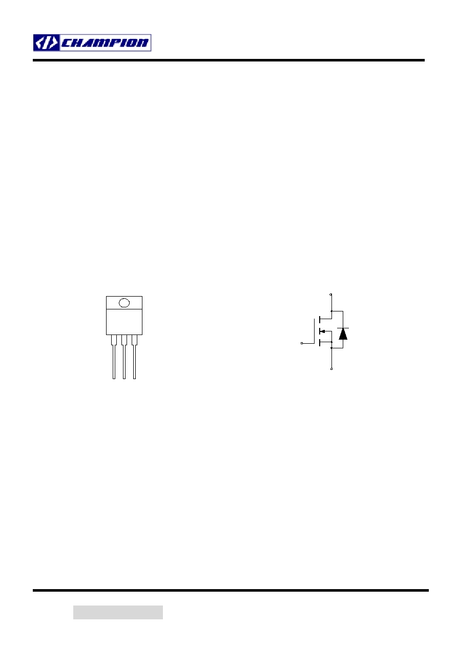
PIN CONFIGURATION
SYMBOL
TO-220/TO-220FP
Front View
1
2
3
GA
T
E
DRA
I
N
S
O
URCE
D
S
G
N-Channel MOSFET
CMT06N60
P
OWER
F
IELD
E
FFECT
T
RANSISTOR
2003/06/19
Preliminary
Rev. 1.1
Champion Microelectronic Corporation
Page 2
ABSOLUTE MAXIMUM RATINGS
Rating Symbol
Value
Unit
Drain to Current Continuous
Pulsed
I
D
I
DM
6.0
18
A
Gate-to-Source Voltage Continue
Non-repetitive
V
GS
V
GSM
±20
±40
V
V
Total Power Dissipation
TO-220
TO-220FP
P
D
125
45
W
Operating and Storage Temperature Range
T
J
, T
STG
-55
to
150
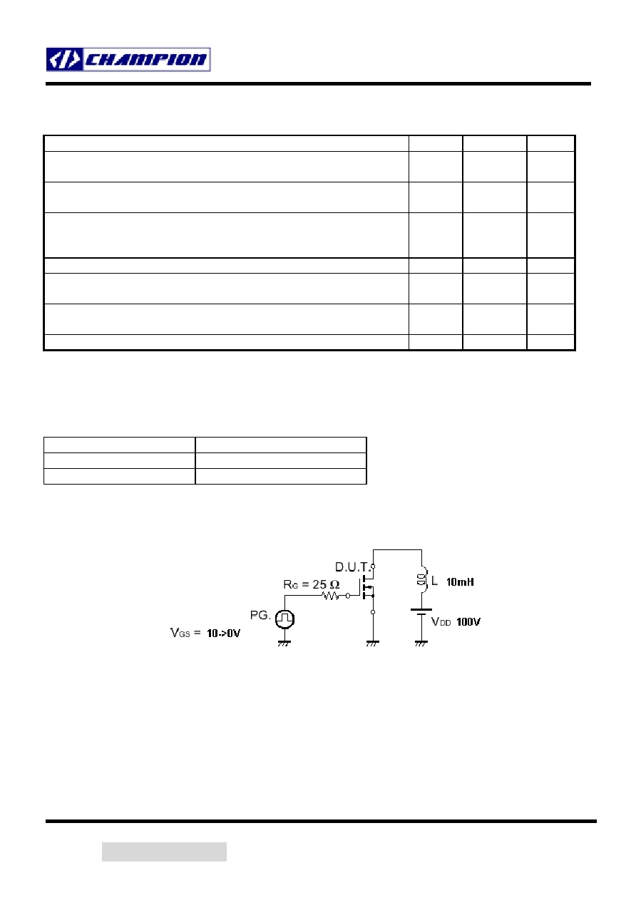
Single Pulse Drain-to-Source Avalanche Energy T
J
= 25
(V
DD
= 100V, V
GS
= 10V, I
L
= 6A, L = 10mH, R
G
= 25)
E
AS
180
mJ
Thermal Resistance Junction to Case
Junction to Ambient
JC
JA
1.0
62.5
/W
Maximum Lead Temperature for Soldering Purposes, 1/8" from case for 10 seconds
T
L
260
(1) VDD = 50V, ID = 6A
(2) Pulse Width and frequency is limited by T
J(max)
and thermal response
ORDERING INFORMATION
Part Number
Package
CMT06N60N220 TO-220
CMT06N60N220FP TO-220FP
TEST CIRCUIT
Test Circuit Avalanche Capability
CMT06N60
P
OWER
F
IELD
E
FFECT
T
RANSISTOR
2003/06/19
Preliminary
Rev. 1.1
Champion Microelectronic Corporation
Page 3
ELECTRICAL CHARACTERISTICS
Unless otherwise specified, T
J
= 25.
CMT06N60
Characteristic Symbol
Min
Typ
Max
Units
Drain-Source Breakdown Voltage
(V
GS
= 0 V, I
D
= 250 A)
V
(BR)DSS
600
V
Drain-Source Leakage Current
(V
DS
= 600 V, V
GS
= 0 V)
(V
DS
= 480 V, V
GS
= 0 V, T
J
= 125)
I
DSS
100
50
A
Gate-Source Leakage Current-Forward
(V
gsf
= 20 V, V
DS
= 0 V)
I
GSSF
100
nA
Gate-Source Leakage Current-Reverse
(V
gsr
= 20 V, V
DS
= 0 V)
I
GSSR
100
nA
Gate Threshold Voltage
(V
DS
= V
GS
, I
D
= 250 A)
V
GS(th)
2.0 4.0 V
Static Drain-Source On-Resistance (V
GS
= 10 V, I
D
= 3.5A) *
R
DS(on)
1.2
Forward Transconductance (V
DS
= 15 V, I
D
= 3.0A) *
g
FS
3.4
mhos
Input Capacitance
C
iss
1498
2100
pF
Output Capacitance
C
oss
158
220
pF
Reverse Transfer Capacitance
(V
DS
= 25 V, V
GS
= 0 V,
f = 1.0 MHz)
C
rss
29
60
pF
Turn-On Delay Time
t
d(on)
14
30
ns
Rise Time
t
r
19
40
ns
Turn-Off Delay Time
t
d(off)
40
80
ns
Fall Time
(V
DD
= 300 V, I
D
= 6.0 A,
V
GS
= 10 V,
R
G
= 9.1) *
t
f
26
55
ns
Total Gate Charge
Q
g
35.5
50
nC
Gate-Source Charge
Q
gs
8.1
nC
Gate-Drain Charge
(V
DS
= 300 V, I
D
= 6.0 A,
V
GS
= 10 V)*
Q
gd
14.1 nC
Internal Drain Inductance
(Measured from the drain lead 0.25" from package to center of die)
L
D
4.5
nH
Internal Drain Inductance
(Measured from the source lead 0.25" from package to source bond pad)
L
S
7.5
nH
SOURCE-DRAIN DIODE CHARACTERISTICS
Forward On-Voltage(1)
V
SD
0.83
1.2
V
Forward Turn-On Time
t
on
** ns
Reverse Recovery Time
(I
S
= 6.0 A,
d
IS
/d
t
= 100A/µs)
t
rr
266
ns
* Pulse Test: Pulse Width 300µs, Duty Cycle 2%
** Negligible, Dominated by circuit inductance
CMT06N60
P
OWER
F
IELD
E
FFECT
T
RANSISTOR
2003/06/19
Preliminary
Rev. 1.1
Champion Microelectronic Corporation
Page 4
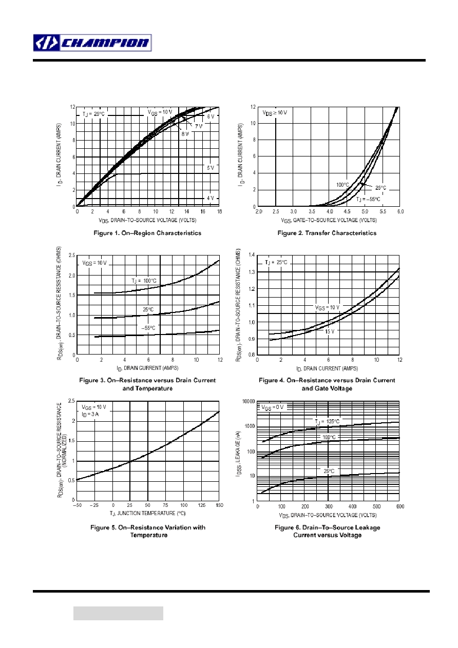
TYPICAL ELECTRICAL CHARACTERISTICS
CMT06N60
P
OWER
F
IELD
E
FFECT
T
RANSISTOR
2003/06/19
Preliminary
Rev. 1.1
Champion Microelectronic Corporation
Page 5
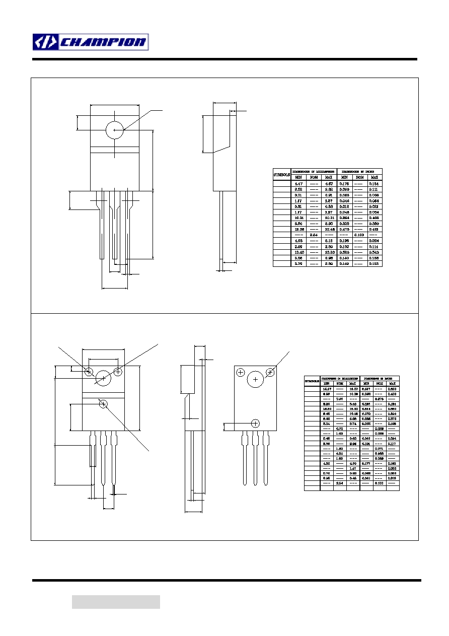
PACKAGE DIMENSION
TO-220
e
e1
D
E
E1
A
b
A1
b1
c
c1
L1
L
F
c1
A
c
A1
D
F
L1
e
b
e1
Front View
Side View
E
E1
L
b1
PIN 1: GATE
PIN 2: DRAIN
PIN 3: SOURCE
TO-220FP
K
M
H
I
J
A
C
B
D
E
G
Q
b
R
b1
P
O
N
M
N
Front View
Side View
Back View
I
J
H
K
C
B
Q
D
E
P
G
b1
b2
e
A
b
O
R
b2
e
R1
.60
R1
.5
0
R1
.50
R3
.18
± 0.
10