�2004 Fairchild Semiconductor Corporation
www.fairchildsemi.com
Rev. 1.0.2
FAN8741 Features
Common
� Built-in thermal shutdown circuit (TSD)
� 8 Independent voltage sources
� Corresponds to 3.3V or 5V DSP
� 4 selectable mute
Spindle
� Output PWM mode control
� FG output: open collector type
� Selectable brake(short & reverse brake)
� Built in hall bias
� 180
o
commutation(compatible with conventional BLDC
spindle motor)
� Built in arm short preventer
BTL(Sled 2-channels)
� Output PWM mode control
� Built in arm short preventer
BTL(Other 4-channels)
� Output LINEAR mode control
Description
The FAN8741G/FAN8742G is a monolithic IC suitable for a
3-phase BLDC(Brush Less Direct Current) spindle motor
driver with PWM, 2-ch motor drivers with PWM for sled
motor and 4-ch linear drivers which drive the focus actuator,
tracking actuator, tilt actuator and loading motor of the opti-
cal media applications. Since FAN8741G/FAN8742G aims
to high-speed/high-density optical media applications its
power stage is made by D-MOS transistors which have
extremely low RDS on. This enables less heat generation
and guarantees more reliable lifetime.
56-SSOP
Typical Applications
� Compact disk ROM (CD-ROM)
� Compact disk RW (CD-RW)
� Digital video disk ROM (DVD-ROM)
� Digital video disk RAM (DVD-RAM)
� Digital video disk Player (DVDP)
� Other compact disk media
� Game console
Ordering Information
X:Tape & Reel type
FAN8741G:FG3X
FAN8742G:FG1X
Device
Package
Operating Temp.
FAN8741G
56-SSOP
-25�C ~ +75�C
FAN8741GX
56-SSOP
-25�C ~ +75�C
FAN8742G
56-SSOP
-25�C ~ +75�C
FAN8742GX
56-SSOP
-25�C ~ +75�C
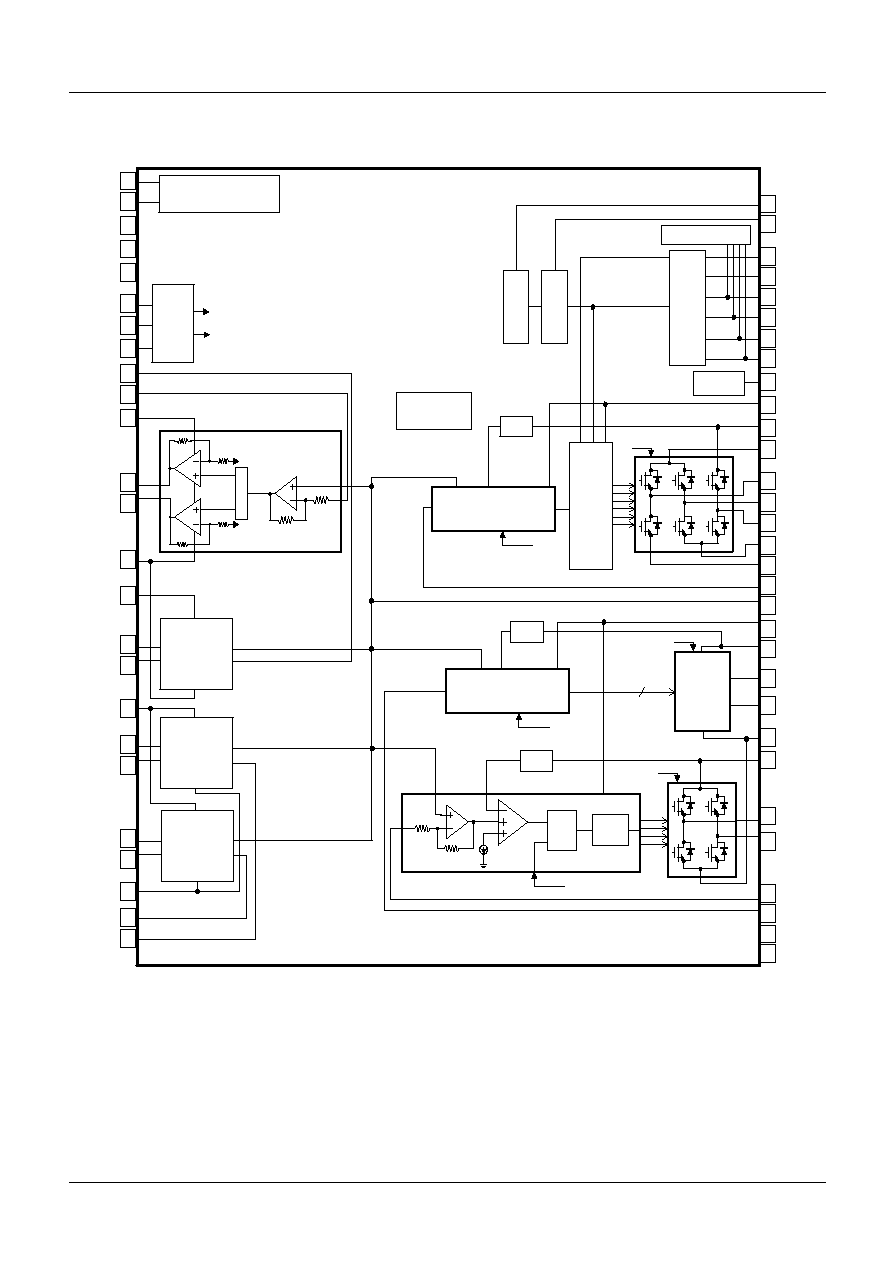
FAN8741/FAN8742
Spindle motor and 6-CH actuator driver
[Spindle(PWM), Sled 2-CH(PWM) 4-CH(Linear)]

FAN8741/FAN8742
3
Pin Definitions
Pin Number
Pin Name
I/O
Pin Function Description
1
DGND
P
Ground for digital block
2
VCP
A
Charge pumped voltage
3
CP2
A
Charge pump capacitor2
4
CP1
A
Charge pump capacitor1
5
SVCC1
P
Power supply for signal block
6
FG
O
Spindle frequency generator
(FAN8741G:3X, FAN8742G:1X)
7
DIR
O
Spindle rotational direction output
8
SPIN
A
Spindle channel input
9
VDD
P
Power supply for digital block
10
IN3
A
Channel 3 input
11
IN4
A
Channel 4 input
12
PGND5
P
Power ground for BTL CH3/4
13
DO4 -
A
Channel 4 drive output -
14
DO4 +
A
Channel 4 drive output +
15
PVCC3
P
Power supply for BTL CH4
16
DO3 -
A
Channel 3 drive output -
17
DO3 +
A
Channel 3 drive output +
18
DO2 -
A
Channel 2 drive output -
19
DO2 +
A
Channel 2 drive output +
20
DO1 -
A
Channel 1 drive output -
21
DO1 +
A
Channel 1 drive output +
22
PGND4
P
Power ground for BTL CH1/2
23
IN1
A
Channel 1 input
24
IN2
A
Channel 2 input
25
PVCC1
P
Power supply for BTL CH1/2
26
PVCC2
P
Power supply for BTL CH3
27
SLIN1
A
Sled channel 1 input
28
SLIN2
A
Sled channel 2 input

FAN8741/FAN8742
4
Pin Definitions(continued)
Pin Number
Pin Name
I/O
Pin Function Description
29
SGND
P
Signal ground for BTL signal block
30
SVCC2
P
Power supply for BTL Pre driver
31
VM2
P
Power supply for sled
32
RSL2
A
Sled current sensing 2
33
RSL1
A
Sled current sensing 1
34
MUTE2
A
Mute input 2
35
MUTE1
A
Mute input 1
36
REF
A
Reference voltage input
37
PGND3
P
Power ground for sled channels
38
SL2-
A
Sled channel 2 drive output -
39
SL2+
A
Sled channel 2 drive output +
40
SL1-
A
Sled channel 1 drive output -
41
SL1+
A
Sled channel 1 drive output +
42
RSP2
A
Spindle current sensing 2
43
W
A
3-phase output W for spindle
44
PGND2
P
Power ground 2 for spindle channel
45
V
A
3-phase output V for spindle
46
RSP1
A
Spindle current sensing 1
47
U
A
3-phase output U for spindle
48
PGND1
P
Power ground 1 for spindle channel
49
VH
A
Hall bias
50
HW-
A
Hall signal input(Hw-)
51
HW+
A
Hall signal input(Hw+)
52
HV-
A
Hall signal input(Hv-)
53
HV+
A
Hall signal input(Hv+)
54
HU-
A
Hall signal input(Hu-)
55
HU+
A
Hall signal input(Hu+)
56
VM1
P
Power supply for spindle