 | ÐлекÑÑоннÑй компоненÑ: FIN24 | СкаÑаÑÑ:  PDF PDF  ZIP ZIP |
FIN24 mSerDes?Low Voltage 24-Bit Bi-Directional Serializer/Deserializer(Preliminary)
Preliminary
© 2005 Fairchild Semiconductor Corporation
DS500887
www.fairchildsemi.com
April 2005
Revised May 2005
FI
N24
P
SerDes
¥
Low
V
o
l
t
age 24-Bi
t Bi-
D
ir
ecti
onal
Ser
i
al
iz
er/
D
e
seri
a
li
zer
(
P
rel
i
minar
y)
FIN24
P
SerDes
¥
Low Voltage 24-Bit Bi-Directional Serializer/Deserializer
(Preliminary)
General Description
The FIN24 allows for a pair of SerDes to interleave data
from two different data sources going opposite directions or
standard bi-directional interface operation. The bi-direc-
tional data flow is controlled through use of a direction
(DIRI) control terminal. The devices can be configured to
operate in a unidirectional mode by only hardwiring the
DIRI terminal. An option for 2 or 4 unidirectional control ter-
minals can be selected by using the S1 and S2 mode con-
trol terminals. An Internal PLL generates the required bit
clock frequency for transfer across the serial link. Options
exist for dual or single PLL operation dependent upon sys-
tem operational parameters. The device has been
designed for low power operation and utilizes Fairchild Low
Power LVDS interface. The device also supports an ultra
low power Power-Down mode for conserving power in bat-
tery operated applications.
Features
s
Low power consumption
s
Low power standards based LVDS differential interface
s
LVCMOS parallel I/O interface
· 2 mA source/sink current
· Over-voltage tolerant control signals
s
I/O Power Supply range between 1.65V and 3.6V
s
Analog Power Supply range of 2.775V
r
5%
s
Multi-Mode operation allows for a single device to
operate as Serializer or Deserializer
s
Internal PLL with no external components
s
Standby Power-Down mode support
s
Built in differential termination
s
Selectable unidirectional control terminals
s
Serialized data rate up to 780Mb/s
s
Small footprint 40-terminal MLP packaging
Ordering Code:
Pb-Free package per JEDEC J-STD-020B.
BGA and MLP packages available in Tape and Reel only.
P
SerDes
¥
is a trademark of Fairchild Semiconductor Corporation.
Order Number
Package Number
Package Description
FIN24GFX
(Preliminary)
BGA42A
Pb-Free 42-Ball Ultra Small Scale Ball Grid Array (USS-BGA), JEDEC MO-195,
3.5mm Wide
FIN24MLX
MLP040A
Pb-Free 40-Terminal Molded Leadless Package (MLP), Quad, JEDEC MO-220, 6mm
Square
Preliminary
www.fairchildsemi.com
2
FIN24
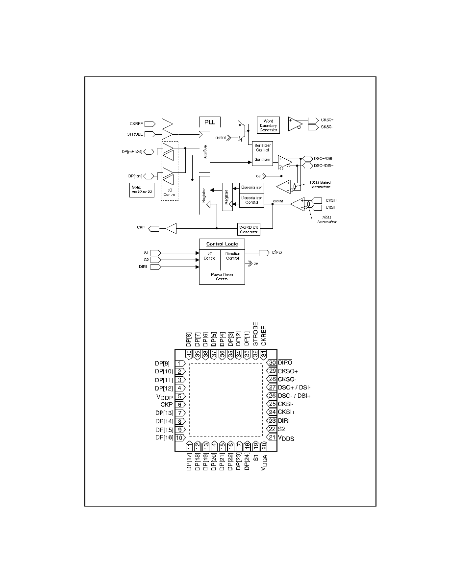
Functional Block Diagram
Connection Diagram
Terminal Assignments for MLP
(Top View)
Preliminary
3
www.fairchildsemi.com
FI
N24
Terminal Description
Note 1: The DSO/DSI serial port terminals have been arranged such that when one device is rotated 180 degrees wrt the other device the serial connections
will properly align without the need for any traces or cable signals to cross. Other layout orientations may require that traces or cables cross.
Control Logic Circuitry
The FIN24 has 4 signals that are selectable as 2 unidirec-
tional inputs and 2 unidirectional outputs, or as 4 unidirec-
tional inputs or 4 unidirectional outputs. These are often
used by applications for control signals. The mode signals
S1 and S2 determine the direction of the DP[21:24] data
signals. The 00 state also provides for a power-down state
where all functionality of the device is disabled or reset.
The DIRI terminal controls whether the device is a serial-
izer or deserializer. When DIRI is asserted LOW, the device
is configured as a 24-bit deserializer. When the DIRI termi-
nal is asserted HIGH, the device will be configured as a
24-bit serializer. Changing the state on the DIRI signal will
reverse the direction of the I/O signals and generate the
opposite state signal on DIRO. For unidirectional operation
the DIRI terminal should be hardwired to the HIGH or LOW
state and the DIRO terminal should be left floating. For bidi-
rectional operation the DIRI of the master device will be
driven by the system and the DIRO signal of the master will
be used to drive the DIRI of the slave device.
When a device with dedicated data outputs turns from a
deserializer to a serializer the dedicated outputs will remain
at the last logical value asserted. This value will only
change if the device is once again turned around into a
deserializer and the values are overwritten.
When operating the SerDes in pairs, not all operating
modes are compatible. Regardless of the mode of opera-
tion the serializer is always sending 24 bits of data and 2
word boundary bits. The deserializer is always receiving 24
bits of data and 2 word boundary bits. For some modes of
operation not all of the data bits are valid due to some pins
being dedicated inputs or outputs. A value of "0" will be
sent for all invalid data bits.
4-Bit Control Mode:
When operating in 4-bit control
mode the master device must be configured
as MODE 2. (S2
1, S1
0) and the slave
device must be configured as MODE 1
(S2
0, S1
1). When operating in this mode
24 data and control bits can be sent from the
master to the slave and 20 data bits can be
sent from the slave to the master. Unidirec-
tional control signals should be connected to
DP[21:24].
2-Bit Control Mode:
When operating in 2-bit control
mode both devices must be configured in
MODE 3 (S2
S1
"1"). In this mode of oper-
ation 22 bits can be sent in either direction.
When operating in a 2-bit control mode serial-
ized bits 21 and 22 will appear on outputs 23
and 24 of the deserializer.
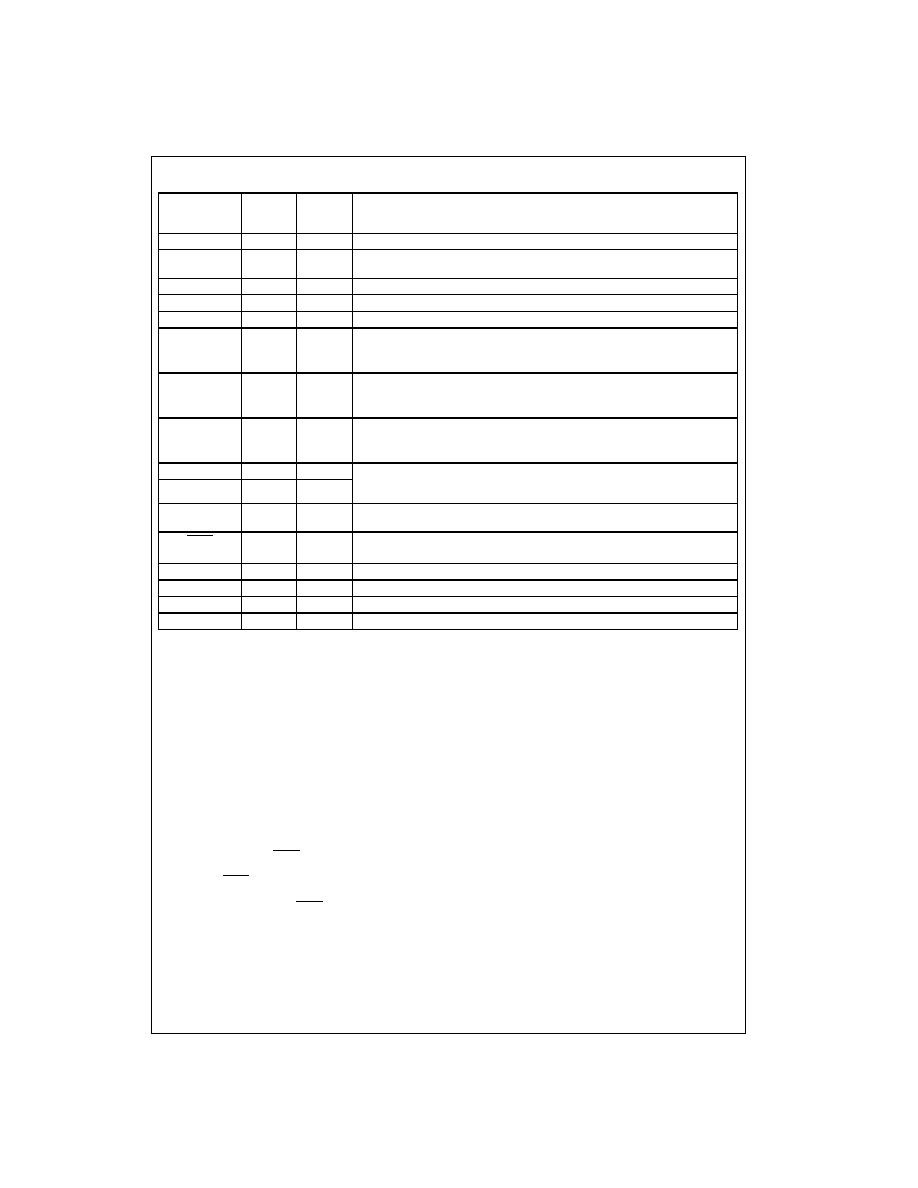
Terminal Name
I/O Type
Number
of
Terminals
Description of Signals
DP[1:20]
I/O
20
LVCMOS Parallel I/O. Direction controlled by DIRI Terminal
DP[21:24]
I or O
4
LVCMOS Parallel Unidirectional Inputs or Outputs Dependent on State of S1, S2
Terminals
CKREF
IN
1
LVCMOS Clock Input and PLL Reference
STROBE
IN
1
LVCMOS Strobe Signal for Latching Data into the Serializer
CKP
OUT
1
LVCMOS Word Clock Output
DSO
/ DSI
DSO
/ DSI
DIFF-I/O
2
LpLVDS Differential Serial I/O Data Signals (Note 1)
DSO: Refers to output signal pair
DSI: Refers to input signal pair
DSO(I)
: Positive signal of DSO(I) pair
DSO(I)
: Negative signal of DSO(I) pair
CKSI
, SKSI
DIFF-IN
2
LpLVDS Differential Deserializer Input Bit Clock
CKSI: Refers to signal pair
CKSI
: Positive signal of CKSI pair
CKSI
: Negative signal of CKSI pair
CKSO
, SKSO
DIFF-OUT
2
LpLVDS Differential Serializer Output Bit Clock
CKSO: Refers to signal pair
CKSO
: Positive signal of CKSO pair
CKSO
: Negative signal of CKSO pair
S1
IN
1
LVCMOS Mode Selection Pins used to define mode of operation for some
terminals. The control terminals, DP[21:24] can be set as 4 terminals in the same
direction or two in each direction.
S2
IN
1
DIRI
IN
1
LVCMOS Control Input
Used to control direction of Data Flow
DIRO
OUT
1
LVCMOS Control Output
Inversion of DIRI
V
DDP
Supply
1
Power Supply for Parallel I/O and Translation Circuitry
V
DDS
Supply
1
Power supply for core circuitry and serial I/O
V
DDA
Supply
1
Power Supply for Analog PLL Circuitry
GND
Supply
0
Use Bottom Ground Plane for Ground Signals
Preliminary
www.fairchildsemi.com
4
FIN24
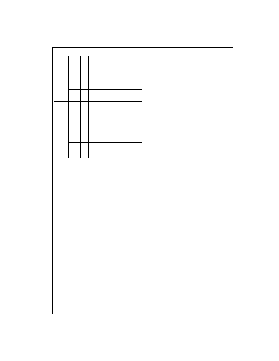
TABLE 1. Control Logic Circuitry
Power-Down Mode: (Mode 0)
Mode 0 is used for powering down and resetting the
device. When both of the mode signals are driven to a
LOW state the PLL and references will be disabled, differ-
ential input buffers will be shut off, differential output buffers
will be placed into a HIGH Impedance state, LVCMOS out-
puts will be placed into a HIGH Impedance state and
LVCMOS inputs will be driven to a valid level internally.
Additionally all internal circuitry will be reset. The loss of
CKREF state is also enabled to insure that the PLL will only
power-up if there is a valid CKREF signal.
In a typical application the device will only change between
the power-down mode and the selected mode of operation.
This allows for system level power-down functionality to be
implemented via a single wire for a SerDes pair. The S1
and S2 selection signals that have their operating mode
driven to a "logic 0" should be hardwired to GND. The S1
and S2 signals that have their operating mode driven to a
"logic 1" should be connected to a system level power-
down signal.
Serializer Operation
The serializer configuration is described in the following
sections. The basic serialization circuitry works essentially
identical in these modes but the actual data and clock
streams will differ dependent on if CKREF is the same as
the STROBE signal or not. When it is stated that CKREF
equals STROBE this means that the CKREF and STROBE
signals are hardwired together as one signal. When it is
stated that CKREF does not equal STROBE then each sig-
nal is distinct and CKREF must be running at a frequency
high enough to avoid any loss of data condition. CKREF
must never be a lower frequency than STROBE.
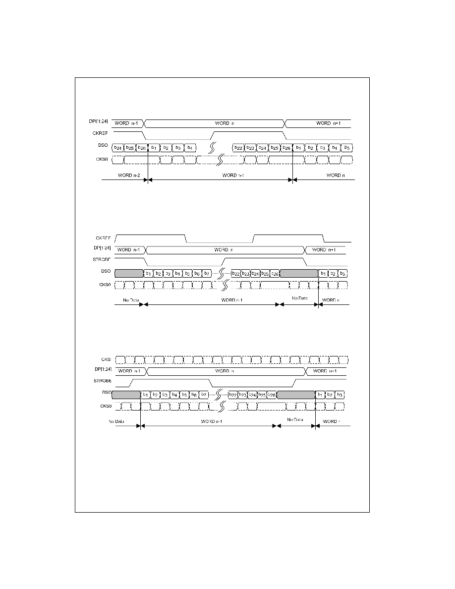
Serializer Operation: (Figure 1)
DIRI equals 1
CKREF equals STROBE
The PLL must receive a stable CKREF signal in order to
achieve lock prior to any valid data being sent. The CKREF
signal can be used as the data STROBE signal provided
that data can be ignored during the PLL lock phase.
Once the PLL is stable and locked the device can begin to
capture and serialize data. Data will be captured on the ris-
ing edge of the STROBE signal and then serialized. The
serialized data stream is synchronized and sent source
synchronously with a bit clock with an embedded word
boundary. Serialized data is sent at 26 times the CKREF
clock rate. Two additional data bits are sent that define the
word boundary. When operating in this mode the internal
deserializer circuitry is disabled including the serial clock,
serial data input buffers, the bidirectional parallel outputs
and the CKP word clock. The CKP word clock will be driven
HIGH.
Serializer Operation: (Figure 2)
DIRI equals 1
CKREF does not equal STROBE
If the same signal is not used for CKREF and STROBE,
then the CKREF signal must be run at a higher frequency
than the STROBE rate in order to serialize the data cor-
rectly. The actual serial transfer rate will remain at 26 times
the CKREF frequency. A data bit value of zero will be sent
when no valid data is present in the serial bit stream. The
operation of the serializer will otherwise remain the same.
The exact frequency that the reference clock needs to run
at will be dependent upon the stability of the CKREF and
STROBE signal. If the source of the CKREF signal imple-
ments spread spectrum technology then the maximum fre-
quency of this spread spectrum clock should be used in
calculating the ratio of STROBE frequency to the CKREF
frequency. Similarly if the STROBE signal has significant
cycle-to-cycle variation then the maximum cycle-to-cycle
time needs to be factored into the selection of the CKREF
frequency.
Serializer Operation: (Figure 3)
DIRI equals 1
No CKREF
A third method of serialization can be done by providing a
free running bit clock on the CKSI signal. This mode is
enabled by grounding the CKREF signal and driving the
DIRI signal HIGH.
At power-up the device is configured to accept a serializa-
tion clock from CKSI. If a CKREF is received then the
device will enable the CKREF serialization mode. The
device will remain in this mode even if CKREF is stopped.
To re-enable this mode the device must be powered down
and then powered back up with "logic 0" on CKREF.
Mode
Number
S2 S1 DIRI
Description
0
0
0
x
Power-Down State. The device will
be powered down and disabled
regardless of all other signals.
1
0
1
0
4-Bit Unidirectional Control Mode
Device operating as a Deserializer
DP[21:24] are outputs
0
1
1
4-Bit Unidirectional Control Mode
Device operating as a Serializer
DP[21:24] are outputs
2
1
0
0
4-Bit Unidirectional Control Mode
Device operating as a Deserializer
DP[21:24] are inputs
1
0
1
4-Bit Unidirectional Control Mode
Device operating as a Serializer
DP[21:24] are inputs
3
1
1
0
2-Bit Unidirectional Control Mode,
Deserializer
DP[21:22] are inputs
DP[23:24] outputs
1
1
1
Unidirectional Control Mode,
Serializer
DP[21:22] are inputs
DP[23:24] outputs
Preliminary
5
www.fairchildsemi.com
FI
N24
Serializer Operation
(Continued)
FIGURE 1. Serializer Timing Diagram (CKREF equals STROBE)
FIGURE 2. Serializer Timing Diagram (CKREF does not equal STROBE)
FIGURE 3. Serializer Timing Diagram Using Provided Bit Clock (No CKREF)