
DOC NO TDS7304-01
REV 1.2
DOC Title
EK7304 DATA SHEET
Page 1 / 1
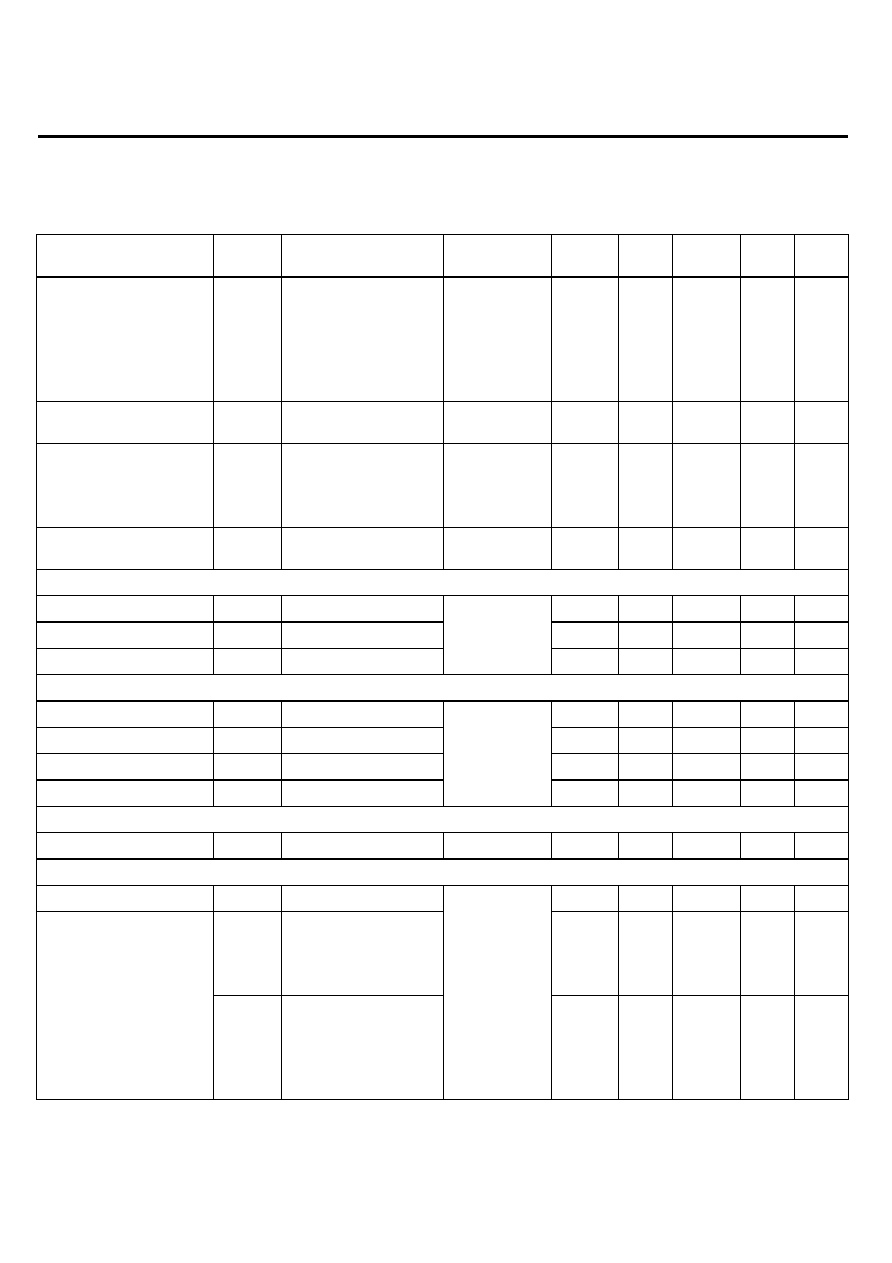
/ Revision History
REV.
REV Date
Eff. Date
REV. Page
//
Revise item / Content
1.0
1.1
1.2
2001/08/29
2001/10/22
2002/07/09
2001/08/29
2001/10/22
2002/07/10
2
3
1112
6
7
1.
Fig.2. Pin Diagram
2.
Pin List
3.
Pin description
1. T
OPR
=-20 to +75
1. OE function
2. XDON function

Microelectronics, Inc.
EK7304
256 Output TFT Gate Driver IC
Eureka
6F, NO.12, INNOVATION 1
ST
. RD.,
SCIENCE-BASED INDUSTRIAL PARK, HSIN-CHU
CITY, TAIWAN, R.O.C.
TEL
886-3-5799255
FAX
886-3-5799253
http://www.eureka.com.tw
CONFIDENTIAL
EUREKA
EK7304
- 1 - Rev 1.2 Jul.09.2002
256- Output TFT Gate Driver IC
DESCRIPTION
The EK7304 is a 256-output TFT gate driver IC
suitable for driving large/medium scale of TFT LCD
panels. Through the use of TCP, it substantially
decreases the size of the frame section of LCD
module.
FEATURES
Output channels:
256 outputs
Driver operating frequency:
max. 1200kHz
LCD drive voltage:
max. V
EE
+43V
Driver output levels: two ("L" level
is changeable)
Incorporates bi-directional shift register.
Supports multi chip operation via output pins.
Pulse width modulation function.
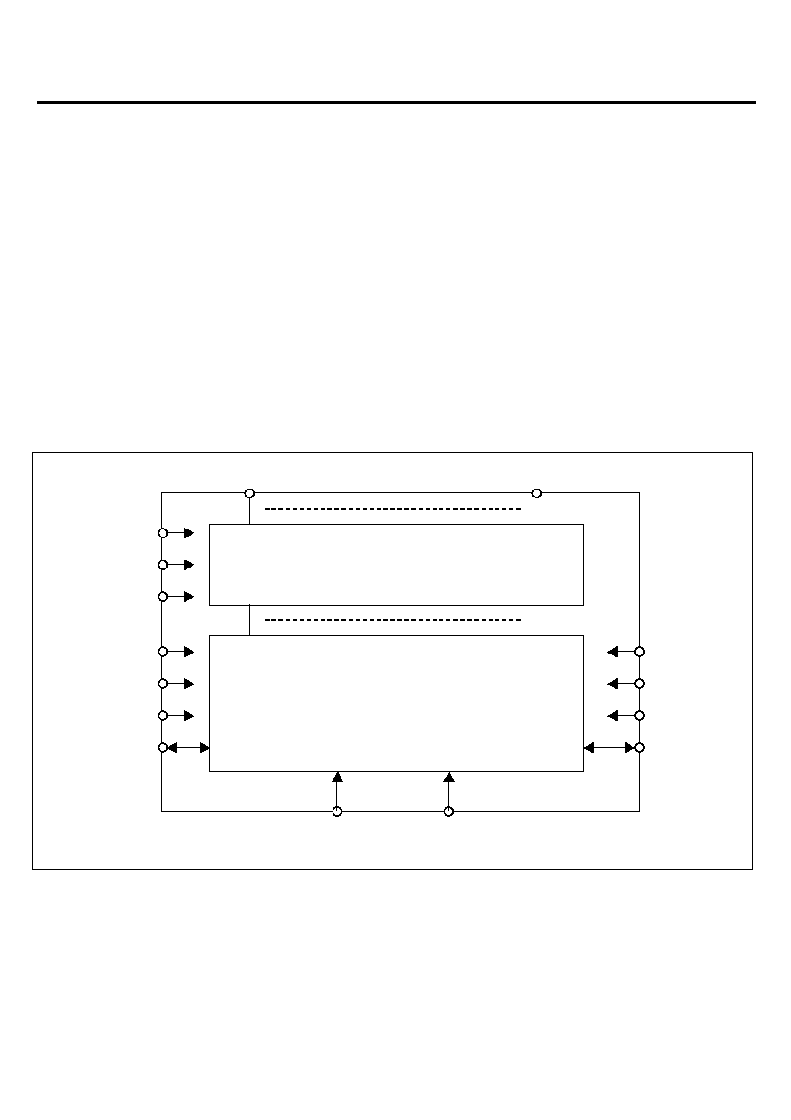
BLOCK DIAGRAM
V
GG
XDON
V
EE
V
DD
V
SS
V
OFF
DIO1
Low voltage logic and IO
High voltage output and level shifters
X
1
X
256
DIO2
OE1
OE2
OE3
FX RL
Fig. 1. Block diagram

CONFIDENTIAL
EUREKA
EK7304
- 2 - Rev 1.2 Jul.09.2002
PINNING INFORMATION
Table 1. Pin List
Terminal Terminal
Name
Terminal Terminal
Name
Terminal Terminal
Name
Terminal Terminal
Name
Terminal Terminal
Name
Terminal Terminal
Name
Terminal Terminal
Name
1
2
3
4
5
6
7
8
9
10
11
12
13
14
15
16
17
18
19
20
21
22
23
24
25
26
27
28
29
30
31
32
33
34
35
36
37
38
39
40
41
42
43
Dummy
X196
X195
X194
X193
X192
X191
X190
X189
X188
X187
X186
X185
X184
X183
X182
X181
X180
X179
X178
X177
X176
X175
X174
X173
X172
X171
X170
X169
X168
X167
X166
X165
X164
X163
X162
X161
X160
X159
X158
X157
X156
X155
44
45
46
47
48
49
50
51
52
53
54
55
56
57
58
59
60
61
62
63
64
65
66
67
68
69
70
71
72
73
74
75
76
77
78
79
80
81
82
83
84
85
86
X154
X153
X152
X151
X150
X149
X148
X147
X146
X145
X144
X143
X142
X141
X140
X139
X138
X137
X136
X135
X134
X133
X132
X131
X130
X129
X128
X127
X126
X125
X124
X123
X122
X121
X120
X119
X118
X117
X116
X115
X114
X113
X112
X111
87
88
89
90
91
92
93
94
95
96
97
98
99
100
101
102
103
104
105
106
107
108
109
110
111
112
113
114
115
116
117
118
119
120
121
122
123
124
125
126
127
128
129
X111
X110
X109
X108
X107
X106
X105
X104
X103
X102
X101
X100
X099
X098
X097
X096
X095
X094
X093
X092
X091
X090
X089
X088
X087
X086
X085
X084
X083
X082
X081
X080
X079
X078
X077
X076
X075
X074
X073
X072
X071
X070
X069
130
131
132
133
134
135
136
137
138
139
140
141
142
143
144
145
146
147
148
149
150
151
152
153
154
155
156
157
158
159
160
161
162
163
164
165
166
167
168
169
170
171
172
X068
X067
X066
X065
X064
X063
X062
X061
Dummy
Dummy
Dummy
Dummy
Dummy
Dummy
Dummy
Dummy
Dummy
Dummy
Dummy
Dummy
Dummy
Dummy
Dummy
Dummy
X060
X059
X058
X057
X056
X055
X054
X053
X052
X051
X050
X049
X048
X047
X046
X045
X044
X043
X042
173
174
175
176
177
178
179
180
181
182
183
184
185
186
187
188
189
190
191
192
193
194
195
196
197
198
199
200
201
202
203
204
205
206
207
208
209
210
211
212
213
214
215
X041
X040
X039
X038
X037
X036
X035
X034
X033
X032
X031
X030
X029
X028
X027
X026
X025
X024
X023
X022
X021
X020
X019
X018
X017
X016
X015
X014
X013
X012
X011
X009
X008
X007
X006
X005
X004
X003
X002
X001
Dummy
VOFF
VEE
216
217
218
219
220
221
222
223
224
225
226
227
228
229
230
231
232
233
234
235
236
237
238
239
240
241
242
243
244
245
246
247
248
249
250
251
252
253
254
255
256
257
258
VEE
VSS
DIO1
RL
FX
OE1
OE2
OE3
DIO2
XDON
VDD
VGG
Dummy
X256
X255
X254
X253
X252
X251
X250
X249
X248
X247
X246
X245
X244
X243
X242
X241
X240
X239
X238
X237
X236
X235
X234
X233
X232
X231
X230
X229
X228
X227
259
260
261
262
263
264
265
266
267
268
269
270
271
272
273
274
275
276
277
278
279
280
281
282
283
284
285
286
287
288
289
290
291
292
293
294
295
296
297
298
299
300
301
302
303
X226
X225
X224
X223
X222
X221
X220
X219
X218
X217
X216
X215
X214
X213
X212
X211
X210
X209
X208
X207
X206
X205
X204
X203
X202
X201
X200
X199
X198
X197
Dummy
Dummy
Dummy
Dummy
Dummy
Dummy
Dummy
Dummy
Dummy
Dummy
Dummy
Dummy
Dummy
Dummy
Dummy
Notes:
1. With the chip name EM7301 orientated normal the pin 1 is in the upper right corner.
2. Counting is anticlockwise.

CONFIDENTIAL
EUREKA
EK7304
- 3 - Rev 1.2 Jul.09.2002
Table 2 Pin description
PIN NO
SYMBOL I/O Function
DESCRIPTION
212 to 154
137 to 2
288 to 229
X
001
-X
256
O
TFT gate driver
output
Under the control of the shift register data, OE1 or OE2 or
OE3, and DIO1 or DIO2, the driver outputs are V
GG
or V
OFF
and change their value at the rising edge of FX
214 V
OFF
Supply
Power supply for TFT driver output low level
215, 216 V
EE
Supply
Negative power supply for Level shifters. Chip ground
217 V
SS
Supply
Logic ground, Reference of the voltages
219 RL
I Shift
direction
selection signal
RL = "H" : X1 X256 (Shift left)
RL = "L" : X256 X1 (Shift right)
DIO1 DIO2
RL = "H"
Input
Output
218
224
DIO1
DIO2
I/O Start pulse input
and output
RL = "L"
Output
Input
225 XDON I Negative
active
input pin
When XDON = "L" then the driver outputs are at the V
GG
level independant of any other input or register value.
220 FX
I Shift
register
clock input
The start pulse is sampled at the rising edge of FX,
The carry pulse changes at the falling edge of FX.
221
222
223
OE1
OE2
OE3
I Negative
active
input pin
When OE
N
= "H" then the associated outputs are set to V
OFF
independent of the register data. This function is not
synchronized with FX.
226 V
DD
Supply
Logic positive power
227 V
GG
Supply
High voltage power and TFT driver output high level

CONFIDENTIAL
EUREKA
EK7304
- 4 - Rev 1.2 Jul.09.2002
FUNCTIONAL DESCRIPTION
Power supply's
The TFT voltage is relative to the logic ground, it can be a negative voltage value.
V
GG
V
DD
V
SS
V
OFF
V
EE
Fig. 2. Relative position of the different supply voltages
Shift direction
The input signals OE1,2,3 and the shift data control the value of the outputs (X
1
till X
256
). Their value can be
either V
GG
or V
OFF
.
The signal LR controls the shift direction of the shift register. The shift register takes its value from one of the
input/output pins DIO at the rising edge of the clock FX and shifts the value to the other input/output pin DIO
where it is presented at the falling edge of FX.
Table 2. RL shift direction relation
RL
Start pulse taken from:
Data shift direction
Output pulse given at:
RL="H" DIO1
X
1
X
256
DIO2
RL="L" DIO2 X
256
X
1
DIO1

CONFIDENTIAL
EUREKA
EK7304
- 5 - Rev 1.2 Jul.09.2002
OE function
When the OE1, OE2, OE3 inputs are "H" than the outputs are driven to V
OFF
regardless of the contents of the
shift register. Each of the three inputs drives it own set of outputs. This function is not synchronized with FX. The
signal XDON can override this function. In the Table below the relation between each OE1,2,3 and their related
outputs is given.
Table 3. OE1,2,3 to Output relation
Non-signal input
Symbol
LCD driver outputs
OE1
X(3i+1) i =0~85
X
1
,X
4
,X
7
,X
10
,
X
247
,X
250
,X
253
,X
256
OE2
X(3i+2) i =0~84
X
2
,X
5
,X
8
,X
11
,
X
248
,X
251
,X
254
OE3
X(3i+3) i =0~84
X
3
,X
6
,X
9
,X
12
,
X
249
,X
252
,X
255
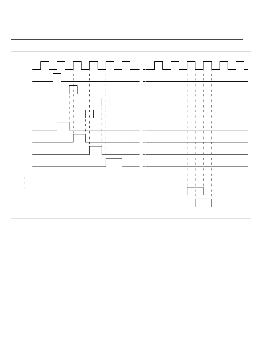
1
2
3
4
5
254
255
256
257
FX
DIO1
OE1
X1
X256
DIO2
X2
X3
X4
OE2
OE3
Fig. 3. OEn Functionality RL= "H"
CONFIDENTIAL
EUREKA
EK7304
- 6 - Rev 1.2 Jul.09.2002
1
2
3
4
5
254
255
256
257
FX
DIO2
OE1
X256
X1
DIO1
X255
X254
X253
OE2
OE3
Fig. 4. OEn Functionality RL= "L"

CONFIDENTIAL
EUREKA
EK7304
- 7 - Rev 1.2 Jul.09.2002
XDON function
When XDON input is "L" then all outputs are driven to the V
GG
level. This function is overriding all other inputs.
With this input all TFT gates are set to high to enable a display off function. This function is not synchronized
with FX.
1
2
3
4
5
254
255
256
257
FX
DIO1
OE1
X1
X256
DIO2
X2
X3
X4
OE2
OE3
XDON
Fig. 5. XDON Functionality RL= "H"

CONFIDENTIAL
EUREKA
EK7304
- 8 - Rev 1.2 Jul.09.2002
CIRCUIT DIAGRAMS
Input/Output Circuit
I
To Internal Circuit
(Applicable pins)
XDON, RL, FX
OE1, OE2, OE3
V
GG
V
EE
V
DD
V
SS
Fig. 6. Input Circuit
I/O
To Internal Circuit
V
GG
(Applicable pins)
DIO1, DIO2
Output Signal
Control Signal
V
DD
V
SS
V
EE
Fig. 7. Input/Output Circuit(1)
CONFIDENTIAL
EUREKA
EK7304
- 9 - Rev 1.2 Jul.09.2002
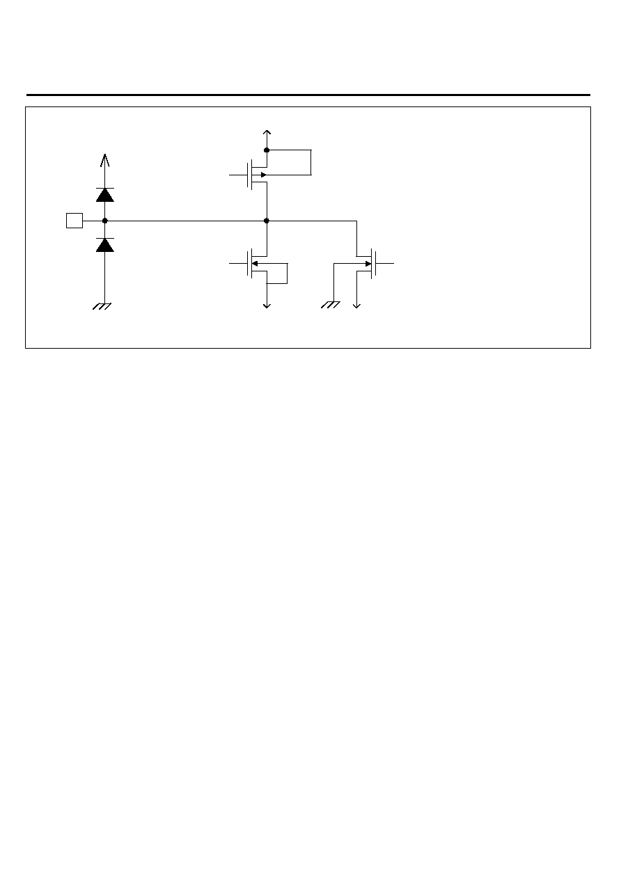
O
Control Signal 3
Control Signal 1
V
EE
V
EE
V
OFF
V
GG
(Applicable pins)
X
1
to X
256
V
EE
V
GG
V
EE
Fig. 8. TFT driver circuit
CONFIDENTIAL
EUREKA
EK7304
- 10 - Rev 1.2 Jul.09.2002
PRECAUTIONS
Precaution when connecting or disconnecting the power supply
This IC has a high-voltage LCD driver, so it may be permanently damaged by a high current which may flow if
voltage is supplied to the LCD driver power supply while the logic system power supply is floating. The detail is
as follows.
When connecting the power supply, connect the LCD drive power after connecting the logic system power.
Furthermore, when disconnecting the power, disconnect the logic system power after disconnecting the LCD
drive power.
ABSOLUTE MAXIMUM RATINGS
Table 4. Absolute maximum Ratings
In accordance with the Absolute Maximum Ratings System (IEC 134); See notes 1 and 2
Parameter Symbol Applicable
Pins
Ratings
Unit NOTE
Supply voltage(1)
V
DD
V
DD
V
SS
-0.3 to +7.0
V
V
GG
V
GG
-0.3 to +45.0
V
V
EE
V
EE
V
GG
-45 to V
GG
+0.3 V
V
OFF
V
OFF
V
EE
-0.3 to V
GG
+0.3 V
V
DD
V
DD
V
EE
-0.3 to V
GG
+0.3 V
Supply voltage(2)
V
SS
V
SS
V
EE
-0.3 to V
GG
+0.3 V
Input voltage
V
I
EO1, EO2, EO3, DIO1
DIO2, RL, FX, XDON
V
SS
-0.3 to V
DD
+0.3
V
EE
-0.3 to V
GG
+0.3
V
1, 2
Storage temperature
T
stg
-45 to +125
Notes:
1. Stress above those listed under Absolute Maximum Ratings may cause permanent damage to the device
2. Parameters are valid over operating temperature range unless otherwise specified.
RECOMMENDED OPERATING CONDITIONS
Table 5. Recommended operating conditions
Parameter
Symbol
Applicable
pins
Min. Typ. Max. Unit NOTE
Supply voltage(1)
V
DD
V
DD
+2.5
+5.5
V
Supply voltage(2)
V
GG
V
GG
+10.0
+42.0
V
Supply voltage(2)
V
EE
V
EE
-25
-5
V
1, 2
Operating temperature
T
OPR
-20
+75
Notes:
1. All voltages are with respect to V
SS
unless otherwise noted (0 V).
2. Ensure that voltages are set such that V
EE
V
SS
<V
DD
<V
GG
. and V
EE
V
OFF
<V
GG
CONFIDENTIAL
EUREKA
EK7304
- 11 - Rev 1.2 Jul.09.2002
ELECTRICAL CHARACTERISTICS
Table 6. DC Characteristics
(V
SS
=0 V, V
DD
=+2.5V to +5.5V, V
GG
=+15.0 to +42.0 V, T
OPR
=-20 to +75 )
Parameter Symbol
Conditions
Applicable
pins
Min. Typ. Max. Unit Note
Operating Supply
Current
I
DD
f
FX
=15.7kHz
f
SL
=60Hz
V
DD
=3.3V
V
EE
=-15V
V
GG
=15V
Output with no load
V
DD
800
�A
Operating Supply
Current
I
GG
V
GG
300
�A
Standby quiescent
supply current
I
DS
Standby
V
DD
=3.3V
V
EE
=-15V
V
GG
=15V
V
DD
600
�A
Standby quiescent
Supply Current
I
GS
V
GG
100
�A
Input pin
H input voltage
V
IH1
0.8xV
DD
V
DD
V
L input voltage
V
IL1
0
0.2xV
DD
V
Input leakage current V
LI1
RL,FX,
OE1~3,
XDON
-10
10
�A
Output pin
H input voltage
V
IH3
0.8xV
DD
V
DD
V
L input voltage
V
IL3
0.2xV
DD
V
H output voltage
V
OH
I
O
= -100 �A
V
DD
-0.4
V
L output voltage
V
OL
I
O
= 100 �A
DIO1,
DIO2
0.4
V
Liquid crystal driving voltage input pin
Input leakage current V
LI2
V
OFF
-100
100
�A
Liquid crystal driving output pin
Output leakage current V
LO1
-50
50 �A
RON-
V
GG
V
GG
=15V
V
EE
=-15V
V
OM
=V
GG
-0.5V
V
OM
is X1~X256
600
1000
Output ON resistance
RON-
V
OFF
V
GG
=15V
V
EE
=-15V
V
OFF
=-10v
V
OM
=V
OFF
+0.5V
V
OM
is X1~X256
X1~X256
600
1000

CONFIDENTIAL
EUREKA
EK7304
- 12 - Rev 1.2 Jul.09.2002
AC Characteristics
(V
SS
= 0 V, V
DD
=+2.5V to +5.5V, V
GG
-V
EE
=+30.0 to +42.0 V, T
OPR
=-20 to +75 )
Parameter Symbol
Conditions
Min.
Typ.
Max.
Unit
Clock period
t
FX
833
ns
Pulse width of clock H level
t
WH
350
ns
Pulse width of clock L level
t
WL
350
ns
DIO data set up time
t
su
50
ns
DIO data hold time
th
350
ns
DIO output delay time
tpd1
CL=50pF
300
ns
Xn output delay time
tpd2
CL=300pF
800
ns
Timing Chart
40%
20% 20%
20%
50%
80% 80%
50%
80%
80%
60%
60%
40%
80%
20%
40%
60%
10%
90%
60%
40%
tpd1 tpd1
tpd2
tpd2
tpd2
tpd2 tpd2
tsu th
tWL tWH
tFX
FX
DIO input
DIO output
Xn
OEm
Xn
XDON
Xn
Fig. 9. Timing

CONFIDENTIAL
EUREKA
EK7304
- 13 - Rev 1.2 Jul.09.2002
DEFINITIONS
Data sheet status
Objective specification This data sheet contains target or goal specifications for product development.
Preliminary
specification
This data sheet contains preliminary data; supplementary data may be published
later.
Product specification
This data sheet contains final product specifications.
Application information
Where application information is given, it is advisory and does not form part of the specification.
LIFE SUPPORT APPLICATIONS
These products are not designed for use in life support appliances, devices, or systems where malfunction of
these products can reasonably be expected to result in personal injury. Eureka customers using or selling these
products for use in such applications do so at their own risk and agree to fully indemnify Eureka for any damages
resulting from such improper use or sale.