
CONFIDENTIAL
Microelectronics,Inc.
EK7402
384-Channel 6-bit Source Driver
for color TFT LCDs
3F,No.7,Industrial East Road 9,Science-Based
Industrial Park, Hsin-Chu, Taiwan, R.O.C
Tel
886-3-5799255
Fax
886-3-5799253
http
//www.eureka.com.tw
Eureka

CONFIDENTIAL
EUREKA
EK7402
- 1 � Rev 1.1 Feb.19.2002
384-Channel 6-bit Source Driver for color TFT LCDs
DESCRIPTION
The EK7402A, EK7402B are 6-bit source driver ICs dedicated for XGA and SXGA TFT-LCD
panels. The digital input is a 6-bit word by 6 dots digital display data, where each word can
generate 64-grayscale levels. By using R/G/B filters 3 dots can be combined to generate a
260'000 colors pixel. Each output can drive alternately 64 positive-polarity or 64 negative-polarity
grayscale levels with respect to the opposite polarity of adjacent odd and even output pins. These
64 positive and negative grayscale levels are generated with 2x5 external reference voltages (V0-
V4, V5-V9) feeding a built-in RDAC that implements a gamma correction for the panel. With
positive and negative output voltage, these circuits feature a dot-dot inversion, n-lines-dot
inversion and frame-dot inversion schemes.
FEATURES
�
CMOS input level (2.3V to 3.6V)
�
High-speed data transfer: F
MAX
= 65 MHz (internal data transfer speed when operating at
V
DD1
= 3.0V)
�
36 data bits (6-bit grayscales code x 3 RGB dot x 2 pixels)
�
Logic power supply voltage (V
DD1
): 2.3V to 3.6V
�
Driver power supply voltage (V
DD2
): 7V to 12V
�
Output dynamic range: V
SS2
+ 0.1V to V
DD2
� 0.1V
�
384 outputs
�
64 positive and negative output voltage levels by means of 2x5 external reference voltages and
a built in D/A converter (R-DAC)
�
Applies for dot-dot inversion, n-line-dot inversion and frame-dot inversion
�
Output voltage polarity inversion function (POL)
�
Bi-directional shift (R/L)
�
Chip-enable signal generation circuit
�
Display data inversion function (POL1, POL2)
�
Low power control function (LPC)
�
Difference point between EK7402A and EK7402B: Gamma correction (Refer to point 11)
CONFIDENTIAL
EUREKA
EK7402
- 2 � Rev 1.1 Feb.19.2002
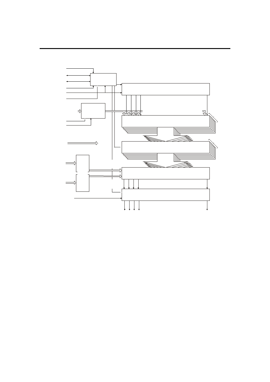
1. INTERNAL
BLOCK
DIAGRAM
LPC
64 bit bidirectional shift register
384 latch circuit (1)
384 latch circuit (2)
384 decoders
384 output Buffers
. . . . . . . . .
. . . . . . . . .
. . . . . . . . .
Control
logic
Data
inversion
circuit
G
r
ay
s
c
a
l
e v
o
l
t
ag
e
g
e
ner
ta
t
i
o
n
V5,V6, V7,
V8, V9
VDD1
VDD2
VSS1
VSS2
S1S2S3S4
S384
POL1
POL2
D -D , D -D
D -D , D -D
D -D , D -D
20
25
30
35
40
45
50
55
STB
STHR
STHL
POL
R/L
CLK
�
�
64 negative-polartiy
Grayscales
6 planes
6 planes
Figure 1: Block diagram
1. Control
logic
unit
Generates the chip-enable signal STHR and STHL and the internal control signals.
2. Data inversion unit
Uses the POL1-POL2 signals to invert or not the 6 x 6-bit input data.
3. 64 bits bi-directional shift register
Generates the enable signals for sequential latching of 64 groups of 36-bit input data.
4. Latch circuit (1)
384x6-bit latch circuits that latch sequentially 6 outputs x 6-bit (2 pixels) from the data bus.
5. Latch circuit (2)
Stores on the rising edge of STB signal the 384x6-bit line data from the first latch stage to
the output buffers.
6. Decoders
Select one of the 64-grayscale levels as a function of the 6-bit code word.
7. Grayscale voltage generation unit
Performs a voltage division of the 10 external input reference voltages, and generates 64
positive-polarity and 64 negative-polarity grayscale levels.
8. Buffers
Drive the selected grayscale voltage level to the panel.