 | –≠–ª–µ–∫—Ç—Ä–æ–Ω–Ω—ã–π –∫–æ–º–ø–æ–Ω–µ–Ω—Ç: HD66137T | –°–∫–∞—á–∞—Ç—å:  PDF PDF  ZIP ZIP |
Document Outline
- Description
- Features
- Pin Arrangement
- Block Diagram
- Internal Block Diagram
- Pin Functions
- Application Example
- Power Supply Circuit Example
- Absolute Maximum Ratings
- Electrical Characteristics
- Terminal Configuration

1
HD66137T
High-Voltage Durable 240-Channel Common Driver
for Dot-Matrix STN LCD
ADE-207-291(Z)
Rev. 2
Aug. 03, 1999
Description
The HD 66137T is a 240-channel common driver which drives a dot matrix STN LCD panel. By changing
the mode, this can be applied to 240- and 200- and 160- channel output. Through the use of a 43-V high-
voltage CMOS process technology, a high-voltage drive of +21.5 V and ≠21.5 V, centering on VM is
possible. ≠21.5V generated from +21.5 V with built-in switching circuit and external capacity. Low logic-
drive voltage (3 V) is used. This device is used together with the segment driver HD66130, HD66134ST or
HD66136.
Features
∑
Display duty: Up to 1/240
∑
LCD drive voltage: 43 V max
∑
Built-in switching circuit (to generate ≠21.5 V)
∑
Number of LCD drive circuit: 240
∑
Operating voltage: 2.5 to 5.5 V
∑
Intermediate voltage I/F
∑
Built-in alternating signal generation circuit Pin programmable
∑
Output mode change: 240-output mode
200-output mode
160-output mode
∑
Built-in display-off function
∑
Flex TCP

HD66137T
2
Pin Arrangement
240 X240
2 X2
1 X1
239 X239
238 X238
237 X237
236 X236
3 X3
4 X4
5 X5
Top view
266
267
265
264
263
262
261
260
259
258
257
256
255
254
253
252
251
250
249
C1
C2
268
VEO
269
VEEL
270
VLL
271
VML
272
VHL
273
VLCDL
DIO2
M
RESET
MWS4
MWS3
MWS2
MWS1
MWS0
VCC
MODE1
MODE0
DOC
DISPOFF
AMP
SHL
GND
CL
248
247
246
245
244
243
242
241
CCL
M
/S
DIO1
VEER
VLR
VMR
VHR
VLCDR
Note: The shape above does not indicate the actual outline.
HD66137T
3
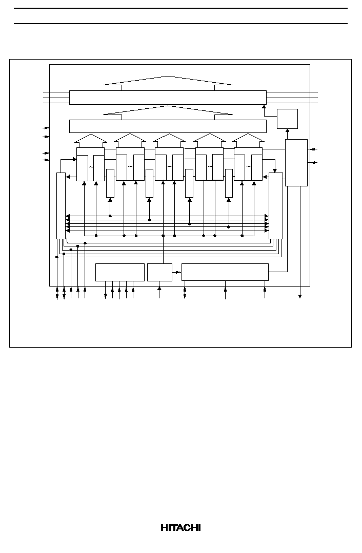
Block Diagram
DISPOFF
*
1 VLCDL and VLCDR, and VEEL and VEER are internally connected.
*
2 VHL and VHR, VLL and VLR, and VML and VMR are internally connected.
DIO2
MODE0
SHL
X1--X240
VHR
VLR
VMR
VCC
GND
Level shifter
VLCDL,R
VEEL,R
*
1,
*
3
*
2,
*
3
VHL
VLL
VML
Level
shifter
Shift register
Shift register
Shift register
Shift register
Shift register
SR
1
D
Q
SR
20
Q
Logic
Logic
DIO1
D
CL
M
Alternating signal
generating circuit
RESET
Logic
DOC
M
/S
LCD drive circuit
MWS 0 to MWS 4
Switch circuit
C2
C1
AMP
VEO
MODE1
SR
21
D
Q
SR
40
Q
D
SR
41
D
Q
SR
200
Q
D
SR
201
D
Q
SR
220
Q
D
SR
221
D
Q
SR
240
Q
D
CCL
Logic
Logic
Logic
Logic
Logic
HD66137T
4
Internal Block Diagram
1. LCD drive Circuit
This circuit selects and outputs the three level signals for the LCD drive. By a combination of the data in
the shift register and M, either VH, VL, or VM is selected and transmitted to the output circuit.
2. Level shifter
This boosts a 5-V signal to a high-voltage signal for LCD drive.
3. Shift register
This is a 240-bit bidirectional shift register circuit. The first line marker signal output from the DIO1 pin
and DIO2 pin is sequentially shifted by shift clock CL. The shift direction is determined by the SHL pin.
4. Alternating signal generating circuit
This circuit generates an alternating signal (M signal) for LCD display. To suppress cross-talk, the signal is
alternated in a unit from several lines to several tens of lines. By connecting MWS0 to MWS4 pins to V
CC
or GND, the desired number of signals can be alternated. When alternating signals are externally input, all
pins (MWS0 to MWS4) are connected to GND.
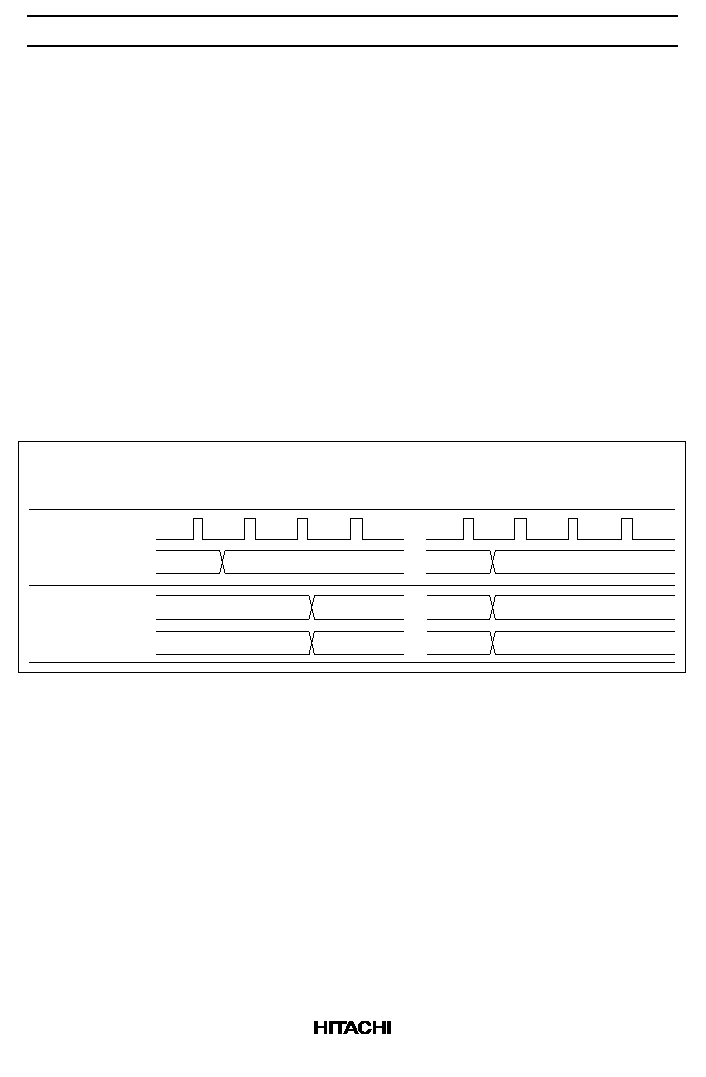
CL1
Input
signal
HIFAS Family timing Comparison
HD66130/131S/134S/135/136
HD66132/133
Output
signal
Segment
M
Common
HD66137T
5
Pin Function
Classification
Symbol
Pin No.
Connected
to
I/O
Functions
Power supply
VLCDL, R
VEEL, R
V
CC
,
GND
273, 241
269, 245
257
250
Power
supply
--
VLCDL, R≠VEEL, R : Power supply for LCD
drive
VLCDL, R : Power supply for switch circuit
V
CC
≠GND : Power supply for logic circuit
VHL, R
VLL, R
VML, R
272, 242
270, 244
271, 243
Power
supply
Input
Power supply for LCD drive level
VHL, R : Selected level (Set to the same
voltage as VLCDL, R.)
VLL, R : Selected level (Set to the same
voltage as VEEL, R.)
VML, R : Non-selected level and Power
supply for switch circuit
VEO
268
VEEL, R
output
When use built -in switching circuit and
generate VEE, VEO pin connect to VEEL, R
pins. VM voltage is point of reference and
reversed and output the voltage input to the
voltage between VLCD and VM. If built-in
switching circuit is not used, don't connect
any lines to this pin.
C1, C2
267, 266 Capacitance --
External capacitance should be connected
here when using the switch circuit for
generate VEE.
If built-in switching circuit is not used, don't
connect any lines to this pin.
Control signal
CL
249
MPU
Input
Shift clock input. Data is shifted at the falling
edge of shift clock CL of the shift register.
M
264
Extension
driver or
MPU
I/O
Inputs or outputs the alternating current for
LCD drive output.
MWS0
MWS1
MWS2
MWS3
MWS4
258
259
260
261
262
--
Input
This pin specifies the cycle of the alternating
signal (M signal) in the unit of the number of
lines. The number of lines, which is an
integer from 2 to 31, is specified as follows.
Usually, specify the number of lines within a
range from 10 to 31. When the HD66131T is
driven by an external alternating signal,
specify the number of lines as zero.
Number
of lines
M-pin status
Line alternating
waveform
MWS4 MWS3 MWS2 MWS1 MWS0
Input
Output
0
0
0
0
∑
∑
1
0
1
2
3
∑
∑
31
0
0
0
0
∑
∑
1
0
0
0
0
∑
∑
1
0
0
1
1
∑
∑
1
0
1
0
1
∑
∑
1
----
Prohibited
2 lines alternated
3 lines alternated
∑
∑
31 lines alternated