Document Outline
- FEATURES
- APPLICATIONS
- CIRCUIT DESCRIPTION
- BLOCK DIAGRAM
- FUNCTIONAL DESCRIPTION
- PIN CONFIGURATION
- FUNCTION BLOCK DESCRIPTION
- INPUT SIGNALS
- OUTPUT SIGNALS
- ELECTRICAL CHARACTERISTICS
- NCO RESET SEQUENCE
- TYPICAL APPLICATION
- SPECTRAL PURITY
- TYPICAL SPECTRUM

R
STEL-1172B
Data Sheet
STEL-1172B
(50 MHz)
32-Bit Resolution
CMOS Numerically
Controlled Oscillator
STEL-1172B
2
FEATURES
s
32 BIT FREQUENCY RESOLUTION
s
PARALLEL SINE AND COSINE
OUTPUTS
s
50 MHz CLOCK FREQUENCY (0∞ TO
70∞C)
s
8-BIT INTERNAL SINE AND COSINE
AMPLITUDE RESOLUTION
s
10-BIT INTERNAL SINE AND COSINE
PHASE RESOLUTION
s
12-BIT PHASE OUTPUT AVAILABLE
s
MILITARY AND COMMERCIAL
TEMPERATURE RANGES AVAILABLE
s
MICROPROCESSOR BUS COMPATIBLE
s
PIN COMPATIBLE WITH ST-1172A
s
CASCADABLE FOR ULTRA HIGH
RESOLUTION
s
LOW POWER CMOS
APPLICATIONS
s
FREQUENCY SYNTHESIZERS
s
HI-SPEED FREQUENCY HOPPED
SOURCES
s
SINGLE SIDEBAND CONVERTERS
s
BASEBAND RECEIVERS
s
DIGITAL SIGNAL PROCESSORS
CIRCUIT DESCRIPTION
The STEL-1172B Numerically Controlled Oscillator
(NCO) generates digital sine and cosine signals of very
precise frequency to be used directly in digital signal
processing applications or in conjunction with a D/A
converter in analog frequency generation applications.
The device, implemented with low power CMOS, can
operate with clock frequencies as high as 50 MHz.
(40 MHz over the military temperature range, 55∞ C to
+125∞ C). The NCO is designed to interface with an
eight bit microprocessor bus.
The NCO maintains a record of phase which is accurate
to 32 bits of resolution. At each clock cycle, the number
stored in the 32 bit
-phase register is added to the
previous value of the phase accumulator. The number
in the phase accumulator represents the current phase of
the synthesized sine and cosine functions. The number in
the
-phase register represents the change of phase for
each cycle of the clock. This number is directly related
to the output frequency by the following:
f
c
x
-Phase
f
o
=
2
32
where: f
o
is the frequency of the output signal
and: f
c
is the clock frequency.
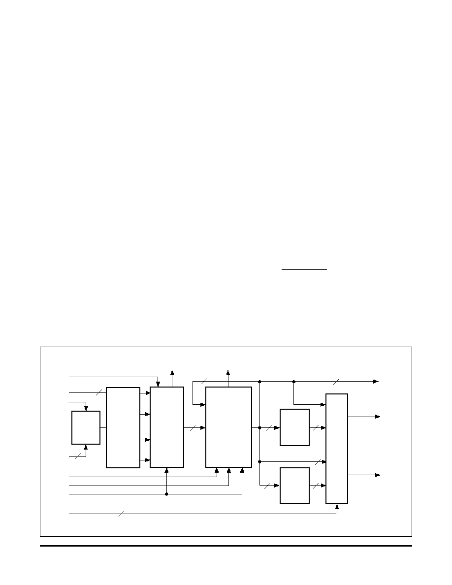
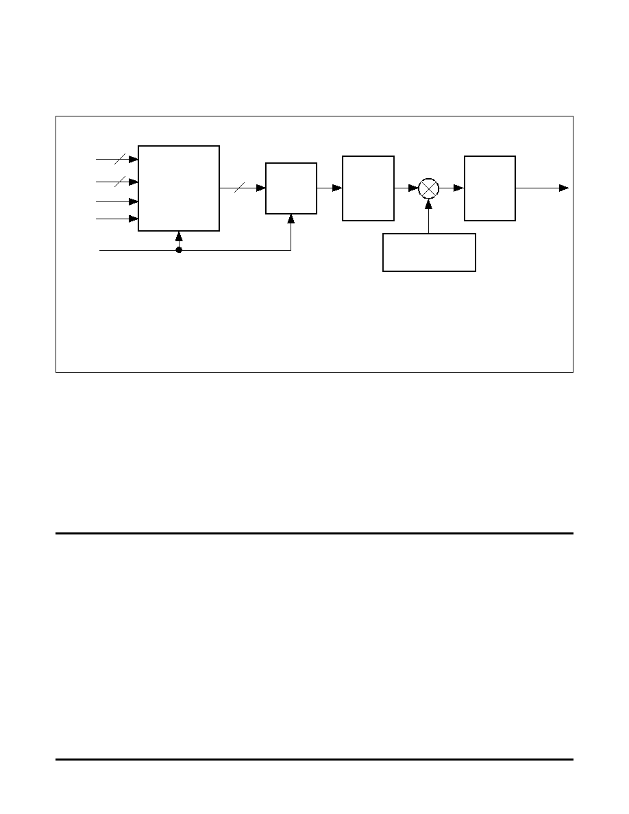
BLOCK DIAGRAM
8
Data
7-0
LDSTB
2
ADDR
1-0
RESET
CLOCK
-PHASE
REGISTER
BLOCK
BUFFER
REGISTER
BLOCK
ADDR.
SELECT
LOGIC
BLOCK
WRN
CARRY IN
SELECT A,B
2
32
32-BIT
PHASE
ACCUMULATOR
BLOCK
32
CARRY OUT
SYNC
10
COSINE
LOOKUP
TABLE
BLOCK
8
8
10
SINE
LOOKUP
TABLE
BLOCK
PHASE
11-4
8
MUX
BLOCK
2
PHASE
3-2
COSINE
7-0
(PHASE
1-0)
SINE
7-0
(PHASE
11-4)
TCP 54836.c
3
STEL-1172B
FUNCTIONAL DESCRIPTION
The sine and cosine signals are generated from
the 10 most significant bits of the phase accumulator.
The frequency of the NCO is determined by the
number stored in the phase register which may be
programmed by an eight-bit microprocessor.
The STEL-1172B NCO generates digitized
sampled sine and cosine signals where the sampling
function is the clock. If the output frequency is very
low with respect to the clock (<f
c
/1024), then the
NCO output will sequence through each of the 1024
states of the sine function stored in the lookup table.
As the output frequency is increased with respect to
the clock, the sine function appears more discontinu-
ous as there are fewer samples in each cycle. At the
Nyquist limit, when the output frequency is exactly half
the clock, the output waveform reduces to a square
wave. The practical upper limit of the NCO output
frequency is about 40% of the clock frequency
because spurious components created by sampling,
which are at a frequency greater than half the clock
frequency, become difficult to remove by filtering.
The phase noise of the NCO output signal may
be determined by knowing the phase noise of the
clock signal input and the ratio of the output fre-
quency to the clock frequency. This ratio squared
times the phase noise power of the clock specified in a
given bandwidth is the phase noise power that may
be expected in that same bandwidth relative to the
output frequency.
The NCO achieves its high operating frequency
by making extensive use of pipelining in its architec-
ture. The pipeline delays within the NCO represent
34 clock cycles. This effectively limits the minimum
possible frequency switching period of the NCO.
After new frequency data is entered the load com-
mand is given. After the 34 cycle pipeline delay the
output will instantaneously switch frequency while
maintaining phase coherence. After this the next new
frequency may be entered. If a 50 MHz clock were
utilized the NCO could be continuously switched
between programmed frequencies with a minimum
practical average switching time of about 1 µsec.
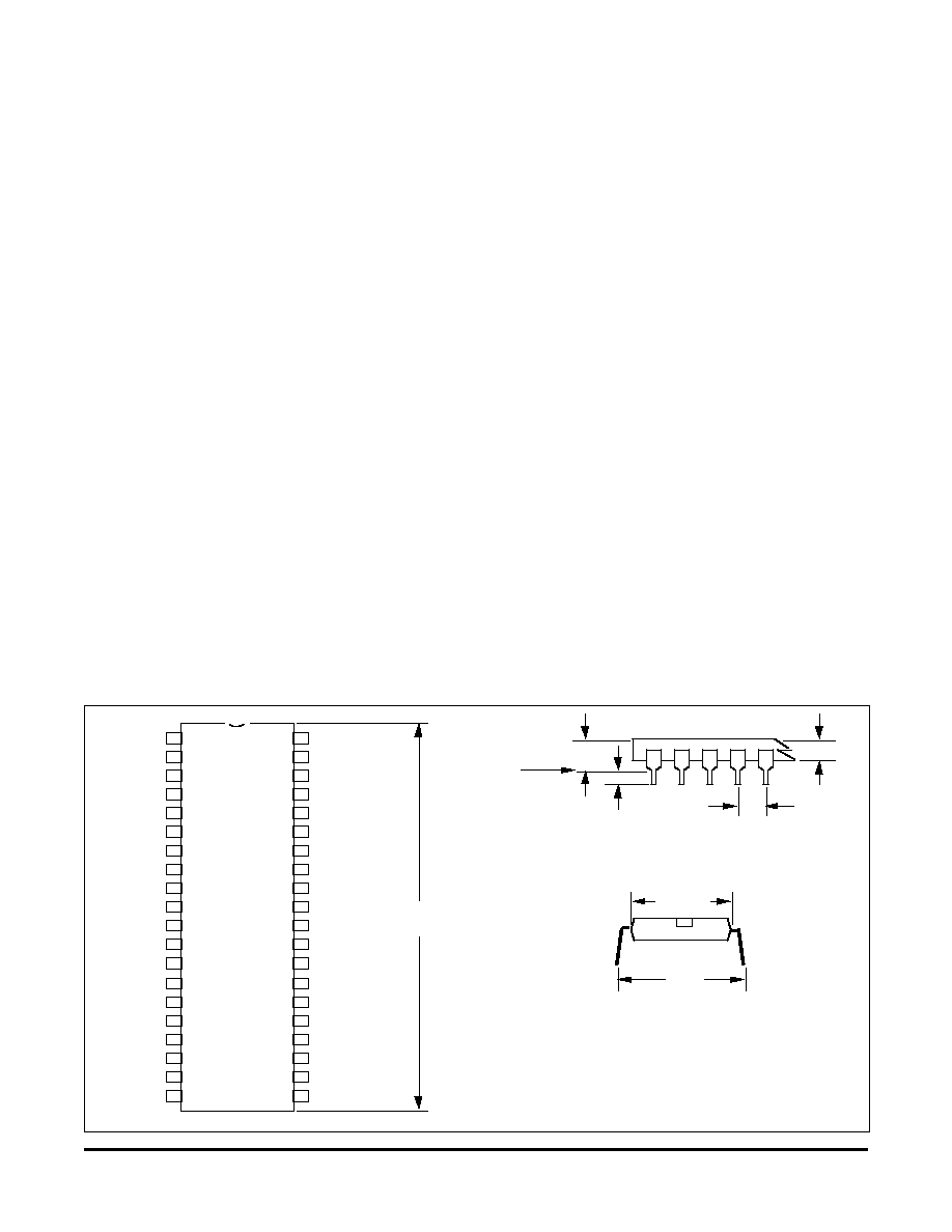
PIN CONFIGURATION
2.00 max.
Seating
plane
0.2"
max.
0.15" typ.
0.13" typ.
0.1" ± 0.01"
Note: tolerance not cumulative
0.55"
typ.
0.6"
(at seating plane)
ADDR
1
COS
5
COS
6
CLOCK
V
SS
COS
2
COS
1
COS
0
SIN
1
SIN
2
SIN
3
SIN
4
SIN
5
SIN
7
COS
7
V
SS
SEL B
PHASE
2
PHASE
3
SEL A
ADDR
0
WRN
LDSTB
CARRY IN
DATA
0
DATA
5
DATA
6
DATA
2
DATA
4
DATA
3
SYNC
DATA
1
DATA
7
RESET
COS
4
V
DD
COS
3
CARRY OUT
SIN
6
SIN
0
1
2
3
4
5
6
7
8
9
10
11
12
13
14
15
16
17
18
19
20
40
39
38
37
36
35
34
33
32
31
30
29
28
27
26
25
24
23
22
21
Package: 40 pin plastic DIP
Thermal coefficient,
jc = 15∞/W
Note: pin spacing for Ceramic
DIP is the same
-
STEL-1172B
4
INPUT SIGNALS
RESET
The RESET input is synchronous with the CLOCK input.
When RESET goes to a logic high level all registers except the
32 bit input buffer and
-Phase register are cleared within 20
nsecs. of the next rising edge of the CLOCK. The output data
and Phase Accumulator are cleared to zero. After the RESET
returns to a logic zero the chip requires 37 rising clock edges to
resume normal operation. For the first two of these cycles the
output data will be 00
H
and then 80
H
, respectively. For the
remaining 35 clock cycles the SIN and COS outputs remain at the
value corresponding to zero phase, i.e. 129, or 81
H
. Normal
operation will then commence, starting at zero phase
CLOCK
All synchronous functions performed within the NCO are
referenced to the rising edge of the CLOCK input. The CLOCK
signal should be nominally a square wave at a maximum
frequency of 50 MHz. A non-repetitive CLOCK waveform is
permissible as long as the minimum duration positive or
negative pulse on the waveform is always greater than 8
nanoseconds. At each rising edge of the CLOCK signal the
contents of the phase accumulator are added to the number
stored in the
-Phase register, and the result is placed in the Phase
Accumulator.
WRN
The information on the 8-bit data bus is transferred to the buffer
register selected by ADDR
1
and ADDR
0
on the falling edge of
the WRN input.
LDSTB
On the rising edge of the clock following the rising edge of the
LDSTB input the information in the four buffer registers is
transferred to the
-Phase Register. The frequency at the NCO
output will change 34 clock cycles after the LDSTB command due
to pipelining delays.
ADDR
1
and ADDR
0
The ADDR
1
and ADDR
0
signals control the use of the DATA
7-0
bus
according to the table:
ADDR
0
ADDR
1
-Phase Register Field
1
1
Bits 0 (LSB) through 7
0
1
Bits 8 through 15
1
0
Bits 16 through 23
0
0
Bits 24 through 31 (MSB)
FUNCTION BLOCK
DESCRIPTION
ADDRESS SELECT LOGIC BLOCK
This block controls the writing of data into the device via the
DATA
7-0
inputs. The data is written into the device on the falling
edge of the WRN input, and the register into which the data is
written is selected by the ADDR
1-0
inputs.
BUFFER REGISTER BLOCK
The Buffer Register is used to temporarily store the
-Phase data
written into the device. This allows the data to be written
asynchronously as four bytes per 32-bit
-Phase word. The data
is transferred from this register into the
-Phase Register after a
rising edge on the LDSTB input.
-PHASE REGISTER BLOCK
This block controls the updating of the
-Phase word used in
the Accumulator. The frequency data from the Mux Block is
loaded into this block after a rising edge on the LDSTB input.
The SYNC output, which indicates the instant of frequency
change at the output at the end of the pipeline delay, is generated
in this block.
PHASE ACCUMULATOR BLOCK
This block forms the core of the NCO function. It is a high-speed,
pipelined, 32-bit parallel accumulator, generating a new sum in
every clock cycle. A carry input (the CARRY IN input) allows the
resolution of the accumulator to be expanded by means of an
auxiliary NCO or phase accumulator. The overflow signal is
discarded (and is available at the CARRY OUT pin), since the
required output is the modulo (2
32
) sum only. This represents
the modulo (2
) phase angle.
SINE AND COSINE LOOKUP TABLE BLOCKS
These blocks are the sine and cosine memories. The 10 most
significant bits from the Phase Accumulator are used to address
this memory to generate the 8-bit SIN
7-0
and COS
7-0
outputs.
MUX BLOCK
The twelve most significant bits from the Phase Accumulator
Block are available at the output via the MUX Blocks as
alternatives to the SIN
7-0
and COS
7-0
outputs. The MUX Blocks
are controlled by the SELECT A and SELECT B inputs.
5
STEL-1172B
OUTPUT SIGNALS
CARRY OUT
Each time the contents of the phase accumulator exceeds the
maximum value that can be represented by a 32 bit number the
CARRY OUT signal goes high for one clock cycle. When two
NCOs are cascaded to obtain 64 bit frequency resolution the
CARRY OUT of the lower order NCO must be connected to
the CARRY IN of the higher order NCO.
SIN
7-0
and COS
7-0
The sine and cosine functions which are presented on the SIN
7-0
and COS
7-0
buses are derived from the 10 most significant bits of
the phase accumulator. The 8-bit sine and cosine functions
are presented in offset binary format with a minimum value of
00
H
and a maximum value of FF
H
. SIN
7
/COS
7
are the MSBs.
When the phase accumulator is zero, the decimal value of the SIN
output is 81
H
. The nominal phase (in degrees) of the sine and
cosine outputs may be determined by multiplying the decimal
equivalent of the ten most significant bits of the phase
accumulator by (360/1024) and adding (360/2048). The average
amplitude over a full cycle is 127.5 decimal. See the description
of SELECT A/B and PHASE for the alternate use of the SIN
7-
0
and COS
7-0
buses.
PHASE
11-0
The twelve most significant bits of the 32 bit phase accumulator
are available as outputs of the NCO. PHASE
11
is the most
significant bit of the 32 bit phase accumulator. The eight most
significant PHASE bits are multiplexed on the SIN bus (see
description of SELECT A input). The next two significant bits
(PHASE
2
and PHASE
3
) are available continuously on pins 18
and 19 respectively. The two least significant bits (PHASE
1
and
PHASE
0
) are multiplexed on the COS bus (see description of
SELECT B input).
SYNC
The normally high SYNC output goes low for one clock cycle 35
rising clock edges after a RESET and 34 rising clock edges after
a LDSTB command. If two NCOs are cascaded for higher
frequency resolution the SYNC output of the lower order NCO
must be connected to the LDSTB input of the higher order
NCO to insure a phase continuous frequency transition.
The least significant bit of the input data bus always maps into
the least significant bit of the
-Phase Register field.
DATA
7
through DATA
0
The eight bit DATA
7-0
bus is used to program the 32 bit
-Phase
Register. DATA
0
is the least significant bit of the bus. To change
all 32 bits of the
-Phase Register, the DATA
7-0
bus must be
sequentially used four times in conjunction with the WRN,
ADDR
0
and ADDR
1
signals.
SELECT A
When SELECT A is a logic 0, the sine function appears on the
SIN
7-0
bus. When SELECT A is a logic 1, the eight most
significant bits of the phase accumulator appear on this bus. The
twelve most significant bits of the 32 bit Phase Accumulator are
available externally. The eight most significant bits appear on the
SIN bus and are labeled PHASE
11
(MSB) through PHASE
4
.
Output Pin
Function:
Function:
Pin
Name SELECT A =0
SELECT A =1
14
SIN
7
SIN
7
(MSB)
PHASE
4
22
SIN
6
SIN
6
PHASE
5
13
SIN
5
SIN
5
PHASE
6
12
SIN
4
SIN
4
PHASE
7
11
SIN
3
SIN
3
PHASE
8
10
SIN
2
SIN
2
PHASE
9
9
SIN
1
SIN
1
PHASE
10
21
SIN
0
SIN
0
(LSB)
PHASE
11
(MSB)
SELECT B
When SELECT B is a logic 1 the two most significant bits of
the cosine function appear on output pins 3 and 15. When Select
B is a logic 0 pin 15 provides the signal PHASE
1
and pin 3
provides the signal PHASE
0
. PHASE
1
and PHASE
0
are the
eleventh and twelfth most significant bits of the phase
accumulator, with PHASE
0
being the least significant accessible
bit.
CARRY IN
Normal operation of the NCO requires that the CARRY IN be
set at a logic 0. When CARRY IN is a logic 1 the effective value
of the
-phase register is increased by one. If two NCOs are
cascaded together to obtain 64 bits of frequency resolution the
CARRY OUT of the lower order NCO is connected to the
CARRY IN of the higher order NCO.
STEL-1172B
6
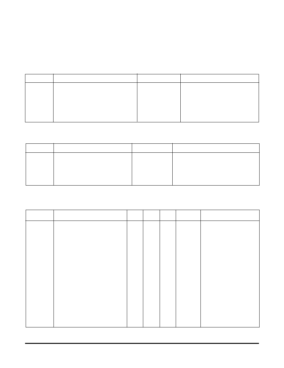
ELECTRICAL CHARACTERISTICS
ABSOLUTE MAXIMUM RATINGS
Warning
: Stresses greater than those shown below may cause permanent damage to the device.
Exposure of the device to these conditions for extended periods may also affect device reliability. All
voltages are referenced to V
SS
.
Symbol
Parameter
Range
Units
T
stg
Storage Temperature
40 to +125
∞C (Plastic package)
65 to +150
∞C (Ceramic package)
V
DDmax
Supply voltage on V
DD
0.3 to + 7
volts
V
I(max)
Input voltage
0.3 to V
DD
+ 0.3
volts
I
i
DC input current
± 10
mA
RECOMMENDED OPERATING CONDITIONS
Symbol
Parameter
Range Units
V
DD
Supply Voltage
+5 ± 5%
Volts (Commercial)
+5 ± 10%
Volts (Military)
T
a
Operating Temperature (Ambient)
0 to +70
∞C
(Commercial)
55 to +125
∞C
(Military)
D.C. CHARACTERISTICS
(Operating Conditions:
V
DD
= 5.0 V ±5%, V
SS
= 0 V, T
a
= 0∞ to 70∞ C, Commercial
V
DD
= 5.0 V ±10%, V
SS
= 0 V, Ta = 55∞ to 125∞ C, Military)
Symbol
Parameter
Min.
Typ.
Max. Units
Conditions
I
DD(Q)
Supply Current, Quiescent
1.0
mA
Static, no clock
I
DD
Supply Current, Operational
3.0 mA/MHz
V
IH(min)
High Level Input Voltage
Standard Operating Conditions
2.0
volts
Logic '1'
Extended Operating Conditions
2.25
volts
Logic '1'
V
IL(max)
Low Level Input Voltage
0.8
volts
Logic '0'
I
IH(min)
High Level Input Current
10
µA
V
IN
= V
DD
I
IL(max)
Low Level Input Current
15
45
130
µA
V
IN
= V
SS
V
OH(min)
High Level Output Voltage
2.4
4.5
volts
I
O
= 4.0 mA
V
OL(max)
Low Level Output Voltage
0.2
0.4
volts
I
O
= +4.0 mA
I
OS
Output Short Circuit Current
20
65
130
mA
V
OUT
= V
DD
, V
DD
= max
10
45
130
mA
V
OUT
= V
SS
, V
DD
= max
C
IN
Input Capacitance
2
pF
All inputs
C
OUT
Output Capacitance
4
pF
All outputs
{
{
{
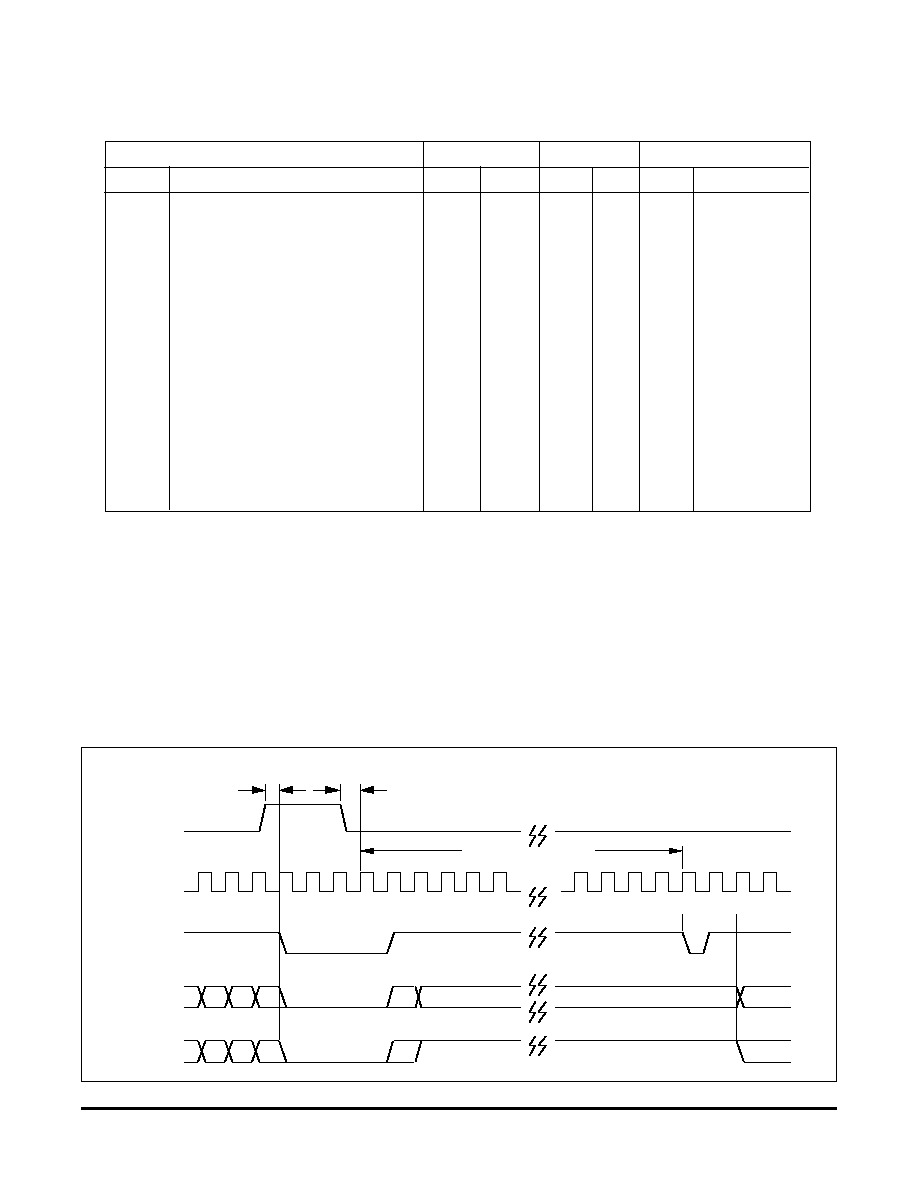
7
STEL-1172B
(Commercial) (Military)
Symbol
Parameter
Min.
Max.
Min. Max. Units Conditions
t
RS
RESET pulse width
30
35
nsec.
t
SR
RESET to CLOCK Setup
10
10
nsec.
t
SU
DATA or ADDR
5
6
nsec.
to WRN Setup, and
LDSTB to CLOCK Setup
t
HD
DATA or ADDR
5
6
nsec.
to WRN Hold, and
LDSTB to CLOCK Hold
t
CH
CLOCK high
8
10
nsec. f
CLK
= max.
t
CL
CLOCK low
8
10
nsec. f
CLK
= max.
t
W
WRN or FRLD pulse width
20
25
nsec.
t
CD
CLOCK to output delay
5
10
3
13 nsec. Load = 15 pF
t
SD
SEL A/B to SIN/COS delay
20
25 nsec. Load = 15 pF
NCO RESET SEQUENCE
00
H
RESET
CLOCK
SYNC
SIN
7-0
35 CLOCK EDGES
81
H
VALID
1
2
3
4
33
34
35
32
80
H
36
37
t
RS
t
SR
00
H
COS
7-0
FF
H
VALID
80
H
A.C. CHARACTERISTICS
(Operating Conditions: V
DD
= 5.0 V ±5%, VSS = 0 V, T
a
= 0∞ to 70∞ C, Commercial
V
DD
= 5.0 V ±10%, VSS = 0 V, Ta = 55∞ to 125∞ C, Military)
STEL-1172B
8
NCO FREQUENCY CHANGE
1
34
2
3
35
SIN/COS
PHASE
NEW
FREQUENCY
OLD
FREQUENCY
35 CLOCK
EDGES
DON'T CARE
DON'T CARE
SELECT A
SELECT B
SIN
7-0,
COS
7-0
LDSTB
SYNC
CLOCK
DATA
7-0
ADDR
1-0
WRN
36
37
DON'T CARE
DON'T CARE
t
SU
t
HD
t
WR
t
CH
t
CL
t
SO
t
CD
t
LS
9
STEL-1172B
SPECTRAL PURITY
In many applications the NCO is used with a digital to
analog converter (DAC) to generate an analog
waveform which approximates an ideal sinewave.
The spectral purity of this synthesized waveform is a
function of many variables including the phase and
amplitude quantization, the ratio of the clock
frequency to output frequency, and the dynamic
characteristics of the DAC.
The sine and cosine signals generated by the
STEL-1172B have eight bits of amplitude resolution
and ten bits of phase resolution which results in
spurious levels which are theoretically about -60 dBc.
The highest output frequency the NCO can generate is
half the clock frequency (f
c
/2), and the spurious
components at frequencies greater than f
c
/2 can be
removed by filtering. As the output frequency f
o
of the
NCO approaches f
c
/2 the "image" spur at f
c
f
o
also
approaches f
c/
2 from above. If the programmed
output frequency is very close to f
c/
2 it will be virtually
impossible to remove this "image" spur by filtering.
For this reason, the maximum practical output
frequency of the NCO should be limited to about 40%
of the clock frequency.
If the STEL-1172B is combined with a high-speed 8-bit video DAC, signals with spectral purity of better
than 55 dBc can be generated up to 10 MHz. In this way a signal can be generated in the 66 to 74 MHz
band after filtering and upconversion. Because of the phase continuous frequency switching
characteristics of the STEL-1172B this architecture is suitable for Frequency Hopping Spread Spectrum
applications.
TYPICAL APPLICATION
HIGH-SPEED HOPPING 66-74 MHz SYNTHESIZER
STEL-1172B
NCO
CLK
8
Data
7-0
2
ADDR
1-0
LDSTB
RESET
CLOCK
8
SINE
D/A
CLK
BPF
2-10
MHz
64 MHz
OSCILLATOR
BPF
66-74
MHz
66-74 MHz
STEL-1172B
1 0
The higher the resolution of the NCO outputs the
greater the spectral purity. Each additional bit used in
quantizing the phase and amplitude of the sine func-
tion (assuming equal resolution for each) provides 6
dB improvement in spectral purity. For this reason, 12
bits of phase information are brought to the STEL-
1172B outputs. It is possible to use these signals with
an external sine ROM to generate sine waves which
have spurious levels as low as -72 dBc.
In some applications the NCO is used with two DACs
to generate analog sine and cosine signals to drive a
single sideband mixer. If the sine and cosine functions
were ideal a typical single sideband mixer would
provide 20 to 30 dB of LO and image suppression. This
performance can be significantly degraded if an NCO
is used to generate these signals near the maximum
NCO frequency. It is recommended that care be taken
when designing the STEL-1172B into such systems
when the output frequency is a significant fraction of
the clock frequency.
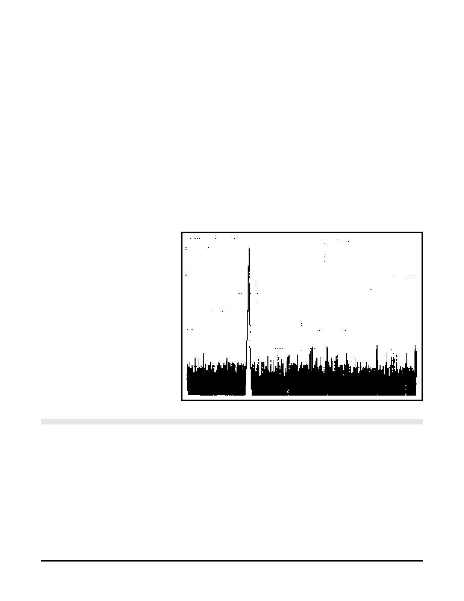
A spectral plot of the NCO output after conversion
with a DAC (AD9703) is shown below. In this case the
clock frequency is 50 MHz and the output frequency is
programmed to 5.6789 MHz. The maximum spur level
observed over the entire useful output frequency
range in this case is 55 dBc. Under other conditions
the spurious levels may be greater than this due to
DAC limitations or clock feedthrough problems
relating to grounding on the PC board. At higher
output frequencies the waveform produced by the
DAC will have large output changes from sample to
sample. For this reason the settling time of the DAC
should be short in comparison to the clock period . As
a general rule the DAC used should have the lowest
possible glitch energy as well as the shortest possible
settling time.
TYPICAL SPECTRUM
Output frequency:
5.6789 MHz
Clock frequency:
50.0 MHz
Frequency Span:
0 to 20 MHz
Reference Level:
0 dBm
Resolution Bandwidth: 1 kHz
Video Bandwidth:
3 kHz
Scale:
Log, 10 dB/div

Copyright © Intel Corporation, December 15, 1999.
All rights reserved
Information in this document is provided in connection with
IntelÆ products. No license, express or implied, by estoppel
or otherwise, to any intellectual property rights is granted by
this document. Except as provided in Intels Terms and Con-
ditions of Sale for such products, Intel assumes no liability
whatsoever, and Intel disclaims any express or implied
warranty, relating to sale and/or use of IntelÆ products in-
cluding liability or warranties relating to fitness for a particu-
lar purpose, merchantability, or infringement of any patent,
copyright or other intellectual property right. Intel products
are not intended for use in medical, life saving, or life sus-
taining applications.
Intel may make changes to specifications and product de-
scriptions at any time, without notice.
For Further Information Call or Write
INTEL CORPORATION
Cable Network Operation
350 E. Plumeria Drive, San Jose, CA 95134
Customer Service Telephone: (408) 545-9700
Technical Support Telephone: (408) 545-9799
FAX: (408) 545-9888