
IRU3065(PbF)
1
www.irf.com
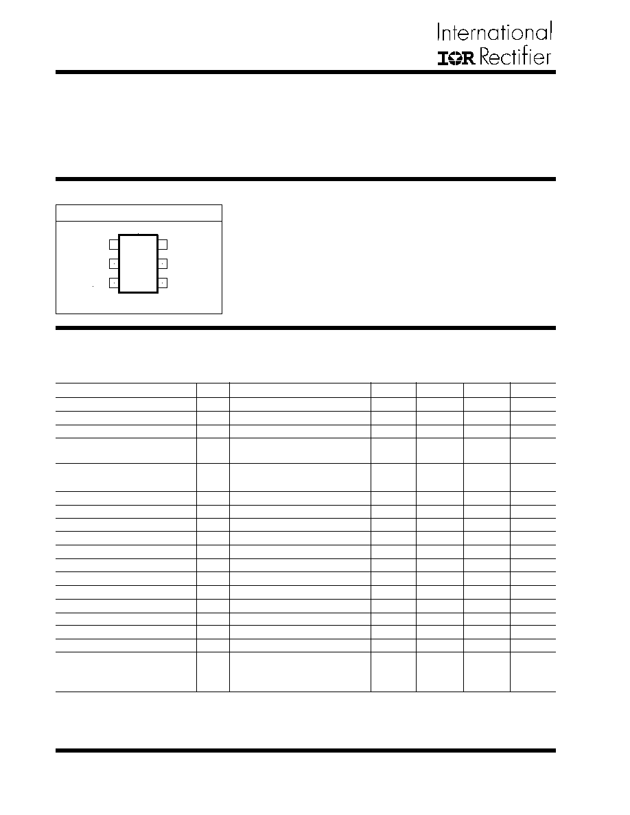
TYPICAL APPLICATION
DESCRIPTION
The IRU3065 controller is designed to provide solutions
for the applications requiring low power on board switch-
ing regulators. The IRU3065 is specifically designed
for positive to negative conversion and uses few com-
ponents for a simple solution. The IRU3065 operates at
high switching frequency (up to 1.5MHz), resulting in
smaller magnetics. The output voltage can be set by
using an external resistor divider. The stability over all
conditions is inherent with this architecture without any
compensation. The device is available in the standard
6-Pin SOT-23.
Generate Negative Output from +5V Input
1A Maximum Output Current
1.5MHz maximum Switching Frequency
Few External Components
Available in 6-Pin SOT-23
FEATURES
APPLICATIONS
Hard Disk Drives
Blue Laser for DVD R-W
MR Head Bias
LCD Bias
GaAs FET Bias
Positive-to-Negative Conversion
Data Sheet No. PD94703 revA
Figure 1 - Typical application of IRU3065 for single input voltage.
POSITIVE TO NEGATIVE DC TO DC CONTROLLER
PRODUCT DATASHEET
V
OUT
= -V
REF
◊
R3
R2
IRU3065
U1
V
DD
Vcc
V
GATE
Gnd
I
SEN
V
SEN
V
OUT
(-5V)
V
REF
= 5V
5V
D1
BAT54
D2
L1
1.2uH
Q1
IRLML5203
R1
0.1
R2
R3
C6
10uF
C3
100pF
10K
10K
10BQ015
C1 1uF
C4
10uF
PACKAGE ORDER INFORMATION
T
A
(
∞
C)
DEVICE PACKAGE OUTPUT VOLTAGE
0 To 70
IRU3065CLTR 6-Pin SOT-23 (L6)
Adjustable
T
A
(
∞
C)
DEVICE PACKAGE OUTPUT VOLTAGE
0 To 70
IRU3065CLTRPbF 6-Pin SOT-23 (L6)
Adjustable
Basic Part (Non Lead-Free)
Lead-Free Part
2
IRU3065(PbF)
www.irf.com
ELECTRICAL SPECIFICATIONS
Unless otherwise specified, these specifications apply over Vcc=5V, V
DD
=7V, C
GATE
=470pF, R
SEN
=0.125,
R
FDBK1
=R
FDBK2
=10K (to Vcc), fs=1.2MHz, I
FL
=0.25A and T
J
=0∞C to 125∞C. Typical values refer to T
J
=25∞C.
ABSOLUTE MAXIMUM RATINGS
Vcc ......................................................................... 7V
V
DD
......................................................................... 12V
Operating Junction Temperature Range ..................... 0∞C To 125∞C
Operating Ambient Temperature Range ..................... 0∞C To 70∞C
Storage Temperature Range ...................................... -65∞C To +150∞C
ESD Capability (Human Body Model) ........................ 2000V
PACKAGE INFORMATION
6-PIN PLASTIC SOT-23 (L6)
PARAMETER SYM TEST CONDITION
MIN TYP MAX UNITS
Recommended Vcc Supply
Recommended V
DD
Supply
Operating Current
Initial Output Voltage Accuracy
Output Accuracy
Voltage Feedback Sense
Voltage Feedback Input Offset
Voltage Feedback Bias Current
Peak Current Sense Voltage
Min Current Sense Voltage
Current Sense Bias Current
Output Drivers Section
Switching Frequency
Max Output Duty Cycle
Min Output Duty Cycle
Rise Time
Fall Time
Propagation Delay from
Current Sense to Output
Note.1
Measured in application
T
J
=25 C, Vout=-5V
Measured in application
over temp. Vout=-5V.
4
4
-1%
-2%
-10
100
5
3
0
145
50
40
40
100
1%
+2%
10
2
2
1.5
0
V
V
mA
V
mV
µA
mV
mV
µA
MHz
%
%
ns
ns
ns
JA
=230 C/W
Vcc
V
DD
Icc
V
V
SEN
V
V
off
I
V
BIAS
V
I
s
V
I
s
I
I
BIAS
fs
Dmax
Dmin
Tr
T
f
T
D
3
2
1
4
5
6
TOP VIEW
Vcc
V
DD
I
SEN
V
GATE
Gnd
V
SEN
Note. 1
Note. 1. guarantted by design
10% to 90% Vgate high
90% to 10% Vgate going low
Vsens=1V. Isens from 0 to
250mV. Delay time between
90% of Isens to 10% of Vgate

IRU3065(PbF)
3
www.irf.com
PIN DESCRIPTIONS
Output driver for external P Channel MOSFET.
This pin serves as ground pin and must be connected to the ground plane.
A resistor divider from this pin to V
OUT
and Vcc or an external V
REF
, sets the output
voltage.
This pin sets the maximum load current by sensing the inductor current.
This pin provides biasing for the output driver.
This pin provides biasing for the internal blocks of the IC.
PIN# PIN SYMBOL PIN DESCRIPTION
1
2
3
4
5
6
V
GATE
Gnd
V
SEN
I
SEN
V
DD
Vcc
BLOCK DIAGRAM
Figure 2 - Simplified block diagram of the IRU3065.
Vcc
V
DD
V
GATE
I
SEN
V
SEN
Gnd
2
3
4
1
5
6
R
S
Q

4
IRU3065(PbF)
www.irf.com
Introduction
The IRU3065 is a controller intended for an inverting
regulator solution. For example, to generate ≠5V from
a 5V supply. The controller is simple and only has a
voltage comparator, current hysteretic comparator, flip-
flop and MOSFET driver. It controls a typical buck boost
converter configured by a P-channel MOSFET, an in-
ductor, a diode and an output capacitor. The sensed
inductor current by a sensing resistor compares with
current comparator. The current comparator uses hys-
teresis to control the turn-on and turn-off of the transis-
tor based upon the inductor current and gated by the
output voltage level. When the inductor current rises
past the hysteresis set point, the output of the current
comparator goes high. The flip-flop is reset and the P-
channel MOSFET is turned off. In the mean time, the
current sense reference is reduced to near zero, giving
a zero reference threshold voltage level. As the induc-
tor current passes below this threshold, which indicates
that the inductor's stored energy has been transferred
to the output capacitor, the current comparator output
goes high and turns on the output transistor (if the out-
put voltage is low). By means of hysteresis, the induc-
tor charges and discharges and functions as self oscil-
lating. The voltage feedback comparator acts as a de-
mand governor to maintain the output voltage at the de-
sired level.
By hysteresis control, the maximum switch current (also
equals inductor current) is limited by the internal cur-
rent sensing reference. The power limit is automatically
achieved. The switching frequency is determined by a
combination of factors including the inductance, output
load current level and peak inductor current. The theo-
retical output voltage and switching frequency versus
output current is shown in Figure 3.
Figure 3 - Theoretical output voltage and switching
frequency vs. output current.
When the output current is below a critical current I
OCP
,
the output voltage is regulated at the desired value and
the switching frequency increases as output current
increases. At current I
OCP
, the switching frequency
reaches its maximum f
S(MAX)
. In this region, the opera-
tion is in regulation mode. When the current goes above
I
OCP
, the operation goes into power limit mode. The out-
put voltage starts to decrease and the output power is
limited. The switching frequency is also reduced.
Analysis shows that the current I
OCP
is determined by:
Where:
Rs = Current Sensing Resistance
VI
SEN(TH)
= Upper Threshold Voltage at the current
comparator (when Vcc=5V, VI
SEN(TH)
=0.145V)
V
IN
= Input Voltage
V
D
= Diode Forward Voltage
V
OUT(NOM)
= Nominal Output Voltage
The maximum switching frequency is determined by:
Where:
I
PEAK
= Peak Inductor Current
I
PEAK
is determined by:
The detailed operation can be seen in the theoretical
operation section
out
I
out
I
Output
voltage
out
V
Switching
frequency
s
f
ocp
I
Regulation
mode
Power limit
mode
max
s
f
APPLICATION INFORMATION
f
S(MAX)
=
V
IN
◊(V
D
-V
OUT(NOM)
)
(V
IN
+V
D
-V
OUT(NOM
)◊L◊I
PEAK
f
S(MAX)
=
V
IN
◊(V
D
-V
OUT(NOM)
)◊R
S
VI
SEN(TH)
◊(V
IN
+V
D
-V
OUT(NOM)
)◊L
---(2)
I
PEAK
= ---(3)
VI
SEN(TH)
R
S
I
OCP
= ◊ ◊ --(1)
1
2
V
IN
V
IN
-V
OUT(NOM)
+V
D
VI
SEN(TH)
Rs

IRU3065(PbF)
5
www.irf.com
Design Example
The following design example is for the evaluation board
application for IRU3065. The schematic is shown in fig-
ure 1:
Voltage Sensing Resistor
The output voltage is determined by the two voltage sens-
ing resistors R2 and R3:
If R3 is chosen as 10K, Then R2 is given by:
Current Sensing Resistor R
S
In order to select R
S
, the desired critical current I
OCP
has to be determined. Considering the switching losses,
for conservative, the critical current should select to be
slightly greater than the nominal output current.
Where 1.5 is the coefficient to take the efficiency into
account.
According to equation (1), the current I
OCP
is given by:
The current sensing resistance is calculated as:
Select R
S
= 0.1
From equation (3), the modified inductor peak current
is:
Where:
V
IN
= 5V
V
OUT(NOM)
= -5V
I
OUT
= 200mA
f
S(MAX)
= Maximum Frequency
f
S(MAX)
= 1.2MHz
V
D
= Diode Forward Voltage
V
D
= 0.5V
Vcc = 5V
VI
SEN(TH)
=145mV
150mV
R2 = - ◊ R3 = - ◊ 10K = 10K
V
REF
V
OUT(NOM)
5V
-5V
I
OCP
= ◊ ◊ = 300mA
1
2
0.15
R
S
V
IN
V
IN
- V
OUT(NOM)
+ V
D
APPLICATION EXAMPLE
V
OUT(NOM)
= - ◊ V
REF
R3
R2
Select:
I
OCP
= 200mA◊1.5 = 300mA
R
S
= ◊ ◊ y 0.12
1
2
0.15
0.3
5
5 - (-5) + 0.5
I
PEAK
= = 1.5A
VI
SEN(TH)
R
S
R
S
= ◊ ◊
1
2
0.15
I
OCP
V
IN
V
IN
- V
OUT(NOM)
+ V
D
I
OCP
= ◊ ◊ 1.5A = 357mA
1
2
5
5 + 0.5
- (-5)
The modified current I
OCP
is:
Output Inductor L
The inductance is chosen by equation (2):
The maximum inductor current is: I
PEAK
= 1.5A
The maximum average inductor current equals
I
AVG
=(VI
SENTH_MAX
+VI
SENTH_MIN
)/Rs/2
I
AVG
=(145mV+50mV)/0.1ohm/2=1A
MOSFET Selection
A P-channel MOSFET is required. The peak current in
this case is equal to I
PEAK
=1.5A. The MOSFET
IRLML5203, from international Rectifier with I
D
=3A and
BVDSS=30V, is a good choice.
Input Capacitor
An input capacitor will help to minimize the induced
ripple on the +5V supply. A 1µF to 10µF X7R ceramic
capacitor is recommended.
Output Capacitor
An output capacitor is required to store energy from
transfer to the output inductor. Its capacitance and ESR
have a great impact on output voltage ripple. A 10µF to
22µF X7R Tantolum or ceramic capacitor is recom-
mended.
Output Diode
The average diode current equals output current. In
this case, select the diode average current larger than
300mA. The lowest block voltage is V
IN
+(-V
OUT
). In this
case, It is 10V. In order to reduce the switching losses,
the Schottky diode is recommended. The diode 10BQ015
from International Rectifier with I
D
=1A and V
BR
=15V is
a good choice.
Other Components
In order to speed up the turn off of P-channel MOSFET,
a fast diode 1N4148 or a 100ohm resistor and 100pF
capacitor is connected to the pin V
DD
and V
GATE
as shown
L
5
1.5A
L ◊ = 1.45µH
V
IN
◊(V
D
- V
OUT(NOM)
)
(V
IN
+V
D
-
V
OUT(NOM)
)◊f
S(MAX)
◊I
PEAK
Select L = 1.2µH
-(-5 - 0.5)
(5 - (-5) + 0.5)◊1.2MHz
I
OCP
= ◊ ◊
1
2
0.15
R
S
V
IN
V
IN
+ V
D
- V
OUT(NOM)