 | ÐлекÑÑоннÑй компоненÑ: IRU3137 | СкаÑаÑÑ:  PDF PDF  ZIP ZIP |
Äîêóìåíòàöèÿ è îïèñàíèÿ www.docs.chipfind.ru

IRU3137
1
Rev. 1.0
06/22/04
www.irf.com
DESCRIPTION
The IRU3137 controller IC is designed to provide a low
cost and high performance synchronous Buck regulator
for on-board DC to DC converter applications. The out-
put voltage can be set as low as 0.8V and higher voltage
can be obtained with an external voltage divider. High
peak current gate drivers provide fast switching transi-
tion for applications requiring high output current in the
range of 15A to 20A.
This device features an internal 200KHz oscillator, un-
der-voltage lockout for both Vcc and Vc supplies, an
external programmable soft-start function as well as
output under-voltage detection that latches off the de-
vice when an output short is detected.
1A Peak Output Drive Capability
0.8V Reference Voltage
Shuts off both drivers at shorted output
and shutdown
Operating with single 5V or 12V supply voltage
Stable with ceramic capacitors
Internal 200KHz Oscillator
Soft-Start Function
Protects the output when control FET is shorted
Synchronous Controller in 8-Pin Package
PACKAGE ORDER INFORMATION
FEATURES
8-PIN SYNCHRONOUS PWM CONTROLLER
APPLICATIONS
DDR Memory Application
Low voltage distributed DC-DC
Graphic Cards
Low cost on-board DC to DC such as 5V to 2.5V,
1.8V or 0.8V
T
A
(°C)
DEVICE PACKAGE FREQUENCY
0 To 70
IRU3137CS 8-Pin Plastic SOIC NB (S) 200KHz
Data Sheet No. PD94700
Figure 1 - Typical application of IRU3137.
TYPICAL APPLICATION
IRU3137
U1
Vcc
Vc
HDrv
LDrv
Fb
Gnd
Comp
SS/SD
C3
1uF
C4
1uF
C8
0.1uF
C9
3300pF
R4
30K
Q1
IRF7832
Q2
IRF7832
R5
1K, 1%
R3
2.15K
L2
2.2uH
L1
1uH
C2
4x 150uF
C1
47uF
2.5V
@ 15A
C7
3x 330uF
40m
, Poscap
12V
5V
Optional
D1
Optional

2
Rev. 1.0
06/22/04
IRU3137
www.irf.com
ABSOLUTE MAXIMUM RATINGS
Vcc Supply Voltage .................................................. -0.5V - 25V
Vc Supply Voltage .................................................... -0.5V - 25V
Storage Temperature Range ...................................... -65°C To 150°C
Operating Junction Temperature Range ..................... 0°C To 125°C
CAUTION: Stresses above those listed in "Absolute Maximum Ratings" may cause permanent damage to the device.
PARAMETER
SYM TEST CONDITION
MIN TYP MAX
UNITS
Fb
Vcc
LDrv
Gnd
HDrv
Vc
Comp
SS
4
3
2
1
5
6
7
8
Reference Voltage
Fb Voltage
Fb Voltage Line Regulation
UVLO
UVLO Threshold - Vcc
UVLO Hysteresis - Vcc
UVLO Threshold - Vc
UVLO Hysteresis - Vc
UVLO Threshold - Fb
UVLO Hysteresis - Fb
Supply Current
Vcc Dynamic Supply Current
Vc Dynamic Supply Current
Vcc Static Supply Current
Vc Static Supply Current
Soft-Start Section
Charge Current
5<Vcc<12
Supply Ramping Up
Supply Ramping Up
Fb Ramping Down
Freq=200KHz, C
L
=3000pF
Freq=200KHz, C
L
=3000pF
SS=0V
SS=0V
SS=0V
0.784
4.0
3.0
0.3
15
0.800
4.25
0.25
3.5
0.25
0.4
0.25
6.5
11
4
2.5
22
0.816
1.6
4.5
3.65
0.5
8
14
6
4
30
V
mV
V
V
V
V
V
V
mA
mA
mA
mA
µ
A
V
FB
L
REG
UVLO Vcc
UVLO Vc
UVLO Fb
Dyn Icc
Dyn Ic
I
CCQ
I
CQ
SS
IB
JA
=160
°
C/W
ELECTRICAL SPECIFICATIONS
Unless otherwise specified, these specifications apply over Vcc=5V, Vc=12V and T
A
=0 to 70°C. Typical values refer
to T
A
=25 C.
PACKAGE INFORMATION
8-PIN PLASTIC SOIC NB (S)

IRU3137
3
Rev. 1.0
06/22/04
www.irf.com
PARAMETER
SYM TEST CONDITION
MIN TYP MAX
UNITS
PIN DESCRIPTIONS
This pin is connected directly to the output of the switching regulator via resistor divider to
provide feedback to the Error amplifier.
This pin provides biasing for the internal blocks of the IC as well as power for the low side
driver. A minimum of 1
µ
F, high frequency capacitor must be connected from this pin to
ground to provide peak drive current capability.
Output driver for the synchronous power MOSFET.
This pin serves as the ground pin and must be connected directly to the ground plane. A
high frequency capacitor (0.1 to 1
µ
F) must be connected from VCC and Vc pins to this
pin for noise free operation.
Output driver for the high side power MOSFET. This pin should not go negative (below
ground), this may cause problem for the gate drive circuit. It can happen when the inductor
current goes negative (Source/Sink), soft-start at no load and for the fast load transient
from full load to no load. To prevent negative voltage at gate drive, a low forward voltage
drop diode might be connected between this pin and ground.
This pin is connected to a voltage that must be at least 4V higher than the bus voltage of
the switcher (assuming 5V threshold MOSFET) and powers the high side output driver. A
minimum of 1
µ
F, high frequency capacitor must be connected from this pin to ground to
provide peak drive current capability.
Compensation pin of the error amplifier. An external resistor and capacitor network is
typically connected from this pin to ground to provide loop compensation.
This pin provides soft-start for the switching regulator. An internal current source charges
an external capacitor that is connected from this pin to ground which ramps up the output
of the switching regulator, preventing it from overshooting as well as limiting the input
current. The converter can be shutdown by pulling this pin below 2.8V.
Error Amp
Fb Voltage Input Bias Current
Fb Voltage Input Bias Current
Transconductance
Oscillator
Frequency
Ramp-Amplitude Voltage
Output Drivers
Rise Time
Fall Time
Dead Band Time
Max Duty Cycle
Min Duty Cycle
SS=3V, Fb=1V
SS=0V, Fb=1V
Note 1
C
L
=3000pF (10% to 90%)
C
L
=3000pF (90% to 10%)
Fb=0.7V, Freq=200KHz
Fb=1.5V
600
180
85
0.1
50
850
1.25
35
35
100
90
µ
A
µ
A
µ
mho
KHz
V
ns
ns
ns
%
%
PIN# PIN SYMBOL PIN DESCRIPTION
1
2
3
4
5
6
7
8
Fb
Vcc
LDrv
Gnd
HDrv
Vc
Comp
SS / SD
I
FB1
I
FB2
GM
Freq
V
RAMP
Tr
T
f
T
DB
T
ON
T
OFF
1100
240
70
70
0
Note 1: Guaranteed by design but not tested in production.

4
Rev. 1.0
06/22/04
IRU3137
www.irf.com
BLOCK DIAGRAM
Figure 2 - Simplified block diagram of the IRU3137.
20uA
64uA Max
POR
Oscillator
Error Amp
Ct
Error Comp
Reset Dom
POR
0.4V
FbLo Comp
Vc
HDrv
Vcc
LDrv
Gnd
Vcc
4.25V
Vc
3.5V
Bias
Generator
3V
0.8V
POR
SS/SD
Fb
Comp
25K
25K
0.8V
3V
R
S
Q
8
1
7
4
3
2
5
6
2.8V
SS
IRU3137
5
Rev. 1.0
06/22/04
www.irf.com
THEORY OF OPERATION
Introduction
The IRU3137 is a fixed frequency, voltage mode syn-
chronous controller and consists of a precision refer-
ence voltage, an error amplifier, an internal oscillator, a
PWM comparator, 1A peak gate driver, soft-start and
shutdown circuits (see Block Diagram).
The output voltage of the synchronous converter is set
and controlled by the output of the error amplifier; this is
the amplified error signal from the sensed output voltage
and the reference voltage.
This voltage is compared to a fixed frequency linear
sawtooth ramp and generates fixed frequency pulses of
variable duty-cycle, which drives the two N-channel ex-
ternal MOSFETs.The timing of the IC is provided through
an internal oscillator circuit which uses on-chip capaci-
tor to set the oscillation frequency to 200 KHz.
Soft-Start
The IRU3137 has a programmable soft-start to control
the output voltage rise and limit the current surge at the
start-up. To ensure correct start-up, the soft-start se-
quence initiates when the Vc and Vcc rise above their
threshold (3.5V and 4.25V respectively) and generates
the Power On Reset (POR) signal. Soft-start function
operates by sourcing an internal current to charge an
external capacitor to about 3V. Initially, the soft-start func-
tion clamps the E/A's output of the PWM converter and
disables the short circuit protection. During the power
up, the output starts at zero and voltage at Fb is below
0.4V. The feedback UVLO is disabled during this time
by injecting a current (64
µ
A) into the Fb. This generates
a voltage about 1.6V (64
µ
A
×
25K) across the negative
input of E/A and positive input of the feedback UVLO
comparator (see Fig3).
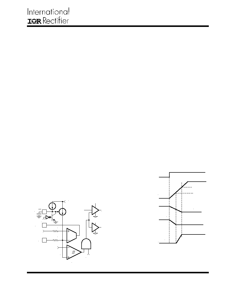
Figure 3 - Soft-start circuit for IRU3137.
The magnitude of this current is inversely proportional to
the voltage at soft-start pin.
The 20
µ
A current source starts to charge up the exter-
nal capacitor. In the mean time, the soft-start voltage
ramps up, the current flowing into Fb pin starts to de-
crease linearly and so does the voltage at the positive
pin of feedback UVLO comparator and the voltage nega-
tive input of E/A.
When the soft-start capacitor is around 1V, the current
flowing into the Fb pin is approximately 32
µ
A. The volt-
age at the positive input of the E/A is approximately:
The E/A will start to operate and the output voltage starts
to increase. As the soft-start capacitor voltage contin-
ues to go up, the current flowing into the Fb pin will keep
decreasing. Because the voltage at pin of E/A is regu-
lated to reference voltage 0.8V, the voltage at the Fb is:
The feedback voltage increases linearly as the injecting
current goes down. The injecting current drops to zero
when soft-start voltage is around 2V and the output volt-
age goes into steady state.
As shown in Figure 4, the positive pin of feedback UVLO
comparator is always higher than 0.4V, therefore, feed-
back UVLO is not functional during soft-start.
Figure 4 - Theoretical operational waveforms
during soft-start.
32
µ
A
×
25K = 0.8V
V
FB
= 0.8-25K
×
(Injected Current)
20uA
64uA
Max
POR
Error Amp
64uA
×
25K=1.6V
When SS=0
POR
0.4V
Feeback
UVLO Comp
SS/SD
Fb
Comp
25K
0.8V
25K
HDrv
LDrv
3V
Soft-Start
Voltage
Voltage at negative input
of Error Amp and Feedback
UVLO comparator
Voltage at Fb pin
Current flowing
into Fb pin
64uA
0uA
0V
0.8V
1.6V
0.8V
0V
3V
2V
1V
Output of UVLO
POR