 | ÐлекÑÑоннÑй компоненÑ: LTC1689IS | СкаÑаÑÑ:  PDF PDF  ZIP ZIP |
1688/89 Layout
1
LTC1688/LTC1689
100Mbps RS485
Hot Swapable Quad Drivers
s
Ultrahigh Speed:
100Mbps
s
Guaranteed Propagation Delay: 8ns
±
4ns
Over Temperature
s
50Mbps Operation with V
DD
= 3V
s
Low Channel-to-Channel Skew: 500ps Typ
s
Low t
PLH
/t
PHL
Skew: 500ps Typ
s
Hot Swap
TM
Capable
s
Driver Outputs Maintain High Impedance in
Three-State or with Power Off
s
Short-Circuit Protected: 3mA Typ Output Current
for an Indefinite Short
s
Thermal Shutdown Protected
s
Single 5V or 3V Supply
s
Pin Compatible with LTC486/LTC487
The LTC
®
1688/LTC1689 are ultrahigh speed, differential
bus/line drivers that can operate at data rates up to
100Mbps. Propagation delay is guaranteed at 8ns
±
4ns
over the full operating temperature range. These devices
operate over the full RS485 common mode range ( 7V
to 12V), and also meet RS422 requirements.
The driver outputs are Hot Swap capable, maintaining
backplane data integrity during board insertion and
removal. The drivers feature three-state outputs, maintain-
ing high impedance over the entire common mode range
( 7V to 12V). Outputs also remain high impedance during
power-up and with the power off. A short-circuit feature
detects bus contention and substantially reduces driver
output current. Thermal shutdown circuitry protects the
parts from excessive power dissipation.
The LTC1688 allows all four drivers to be enabled together,
while the LTC1689 allows two drivers at a time to be
enabled.
The LTC1688/LTC1689 operate from a single 5V or 3V
supply and draw only 9mA of supply current.
s
High Speed RS485 Twisted-Pair Drivers
s
High Speed Backplane Drivers
s
Complementary Clock Drivers
s
STS-1/OC-1 Data Drivers
s
SCSI Drivers
Hot Swap is a trademark of Linear Technology Corporation.
, LTC and LT are registered trademarks of Linear Technology Corporation.
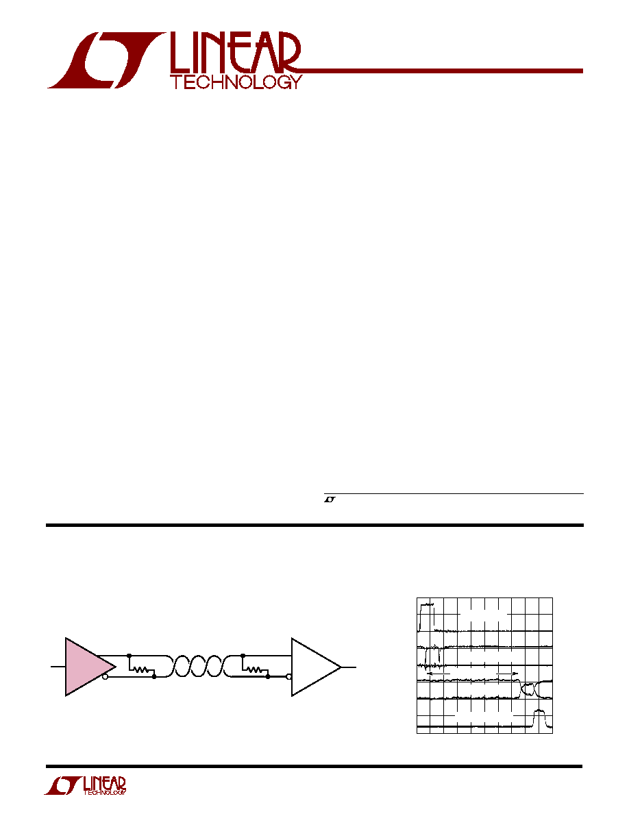
20ns Pulse Across 100 Feet
of Category 5 UTP
20ns/DIV
2V/DIV
2V/DIV
2V/DIV
5V/DIV
1688/89 TA02
DRIVER INPUT
DRIVER OUTPUTS
RECEIVER INPUT
RECEIVER OUTPUT
CABLE DELAY
1688/89 TA01
RECEIVER
1/4 LTC1688
100
100
1/4 LTC1518
100 FT CATEGORY 5 UTP
DRIVER
50Mbps RS485 Data Connection
DESCRIPTIO
U
FEATURES
APPLICATIO S
U
TYPICAL APPLICATIO
U
2
LTC1688/LTC1689
W
U
U
PACKAGE/ORDER I FOR ATIO
A
U
G
W
A
W
U
W
A
R
BSOLUTE
XI
TI
S
(Note 1)
Supply Voltage (V
DD
) ................................................ 7V
Enable Input Voltages ................. 0.5V to (V
DD
+ 0.5V)
Enable Input Currents ..................... 100mA to 100mA
Driver Input Voltages .................. 0.5V to (V
DD
+ 0.5V)
Driver Output Voltages ................. ( 12V + V
DD
) to 12V
Driver Input Currents ...................... 100mA to 100mA
Short-Circuit Duration (V
OUT
: 7V to 10V) ...... Indefinite
Operating Temperature Range
LTC1688C/LTC1689C ............................. 0
°
C to 70
°
C
LTC1688I/LTC1689I .......................... 40
°
C to 85
°
C
Storage Temperature Range ................ 65
°
C to 150
°
C
Lead Temperature (Soldering, 10 sec)................. 300
°
C
DC ELECTRICAL CHARACTERISTICS
SYMBOL
PARAMETER
CONDITIONS
MIN
TYP
MAX
UNITS
V
DD
= 5V, Per Driver, T
A
= 25
°
C, Unless Otherwise Noted (Note 2)
V
OD1
Differential Driver Output (Unloaded)
I
OUT
= 0
q
V
DD
V
V
OD2
Differential Driver Output (With Load)
R = 50
(RS422)
q
2
V
R = 25
(RS485), Figure 1
q
1.5
3.0
V
V
OD
Change in Magnitude of Driver Differential
R = 25
or 50
, Figure 1
q
0.2
V
Output Voltage for Complementary
Output States
V
OC
Driver Common Mode Output Voltage
R = 25
or 50
, Figure 1
q
2
3
V
V
OC
Change in Magnitude of Driver Common
R = 25
or 50
, Figure 1
q
0.2
V
Mode Output Voltage for Complementary
Output States
V
IH
Input High Voltage
EN, ENB, EN12, EN34, DI
q
2
V
V
IL
Input Low Voltage
EN, ENB, EN12, EN34, DI
q
0.8
V
I
IN1
Input Current
EN, ENB, EN12, EN34, DI
q
±
1
µ
A
I
OZ
Three-State (High Impedance)
V
OUT
= 7V to 12V
q
±
2
±
200
µ
A
Output Current
I
DD
Supply Current of Entire Device
No Load, Digital Input Pins = 0V or V
DD
q
9
18
mA
I
OSD1
Driver Short-Circuit Current, V
OUT
= HIGH
V
OUT
= 7V to 10V
q
±
20
mA
I
OSD2
Driver Short-Circuit Current, V
OUT
= LOW
V
OUT
= 7V to 10V
q
±
20
mA
V
DD
= 3V, Per Driver, T
A
= 25
°
C, Unless Otherwise Noted (Note 2)
V
OD1
Differential Driver Output (Unloaded)
I
OUT
= 0
q
V
DD
V
V
OD2
Differential Driver Output (With Load)
R = 50
(RS422)
1.5
V
R = 25
(RS485), Figure 1
q
0.65
2.0
V
V
OD
Change in Magnitude of Driver Differential
R = 25
or 50
, Figure 1
0.1
V
Output Voltage for Complementary
Output States
V
OC
Driver Common Mode Output Voltage
R = 25
or 50
, Figure 1
1.3
V
ORDER PART
NUMBER
LTC1688CS
LTC1689CS
LTC1688IS
LTC1689IS
TOP VIEW
S PACKAGE
16-LEAD PLASTIC SO
*LTC1689 ONLY
1
2
3
4
5
6
7
8
16
15
14
13
12
11
10
9
DI1
DO1A
DO1B
EN (EN12*)
DO2B
DO2A
DI2
GND
V
DD
DI4
DO4A
DO4B
ENB (EN34*)
DO3B
DO3A
DI3
T
JMAX
= 150
°
C,
JA
= 90
°
C/ W
The
q
denotes the specifications which apply over the full operating
temperature range, otherwise specifications are at T
A
= 25
°
C.
Consult factory for parts specified with wider operating temperature ranges.
3
LTC1688/LTC1689
SYMBOL
PARAMETER
CONDITIONS
MIN
TYP
MAX
UNITS
V
OC
Change in Magnitude of Driver Common
R = 25
or 50
, Figure 1
0.1
V
Mode Output Voltage for Complementary
Output States
V
IH
Input High Voltage
EN, ENB, EN12, EN34, DI
q
1.4
V
V
IL
Input Low Voltage
EN, ENB, EN12, EN34, DI
q
0.5
V
I
IN1
Input Current
EN, ENB, EN12, EN34, DI (Note 3)
q
±
1
µ
A
I
OZ
Three-State (High Impedance)
V
OUT
= 7V to 10V (Note 3)
q
±
1
±
200
µ
A
Output Current
I
DD
Supply Current of Entire Device
No Load, Digital Input Pins = 0V or V
DD
5
mA
I
OSD1
Driver Short-Circuit Current, V
OUT
= HIGH
V
OUT
= 7V to 8V (Note 3)
q
±
20
mA
I
OSD2
Driver Short-Circuit Current, V
OUT
= LOW
V
OUT
= 7V to 8V (Note 3)
q
±
20
mA
Note 1: Absolute Maximum Ratings are those values beyond which the life
of a device may be impaired.
Note 2: All currents into the device pins are positive; all currents out of the
device pins are negative.
Note 3: Guaranteed by design or correlation, but not tested.
SWITCHI
N
G CHARACTERISTICS
U
SYMBOL
PARAMETER
CONDITIONS
MIN
TYP
MAX
UNITS
V
DD
= 5V, T
A
= 25
°
C, Unless Otherwise Noted (Note 2)
t
PLH
, t
PHL
Driver Input-to-Output Propagation Delay
R
DIFF
= 50
, C
L1
= C
L2
= 25pF,
q
4
8
12
ns
Figures 2, 4
t
SKEW
Driver Output-to-Output Skew
R
DIFF
= 50
, C
L1
= C
L2
= 25pF,
500
ps
Figures 2, 4
t
r
, t
f
Driver Rise/Fall Time
R
DIFF
= 50
, C
L1
= C
L2
= 25pF,
2
ns
Figures 2, 4
t
ZH
Driver Enable to Output High
C
L
= 25pF, S2 Closed, Figures 3, 5
q
10
35
ns
t
ZL
Driver Enable to Output Low
C
L
= 25pF, S1 Closed, Figures 3, 5
q
10
35
ns
t
LZ
Driver Disable from Low
C
L
= 15pF, S1 Closed, Figures 3, 5
q
25
65
ns
t
HZ
Driver Disable from High
C
L
= 15pF, S2 Closed, Figures 3, 5
q
25
65
ns
C
L(MAX)
Maximum Output Capacitive Load
(Note 3)
q
200
pF
Maximum Data Rate
(Note 3)
q
100
Mbps
Maximum Driver Input Rise/Fall Time
(Note 3)
q
500
ns
V
DD
= 3V, T
A
= 25
°
C, Unless Otherwise Noted (Note 2)
t
PLH
, t
PHL
Driver Input-to-Output Propagation Delay
R
DIFF
= 50
, C
L1
= C
L2
= 25pF,
11
ns
Figures 2, 4
t
SKEW
Driver Output-to-Output Skew
R
DIFF
= 50
, C
L1
= C
L2
= 25pF,
1
ns
Figures 2, 4
t
r
, t
f
Driver Rise/Fall Time
R
DIFF
= 50
, C
L1
= C
L2
= 25pF,
4
ns
Figures 2, 4
t
ZH
Driver Enable to Output High
C
L
= 25pF, S2 Closed, Figures 3, 5
25
ns
t
ZL
Driver Enable to Output Low
C
L
= 25pF, S1 Closed, Figures 3, 5
25
ns
t
LZ
Driver Disable from Low
C
L
= 15pF, S1 Closed, Figures 3, 5
50
ns
t
HZ
Driver Disable from High
C
L
= 15pF, S2 Closed, Figures 3, 5
50
ns
C
L(MAX)
Maximum Output Capacitive Load
(Note 3)
q
200
pF
Maximum Data Rate
50
Mbps
Maximum Driver Input Rise/Fall Time
(Note 3)
q
500
ns
DC ELECTRICAL CHARACTERISTICS
The
q
denotes the specifications which apply over the full operating
temperature range, otherwise specifications are at T
A
= 25
°
C.
The
q
denotes the specifications which apply over the full operating
temperature range, otherwise specifications are at T
A
= 25
°
C.
4
LTC1688/LTC1689
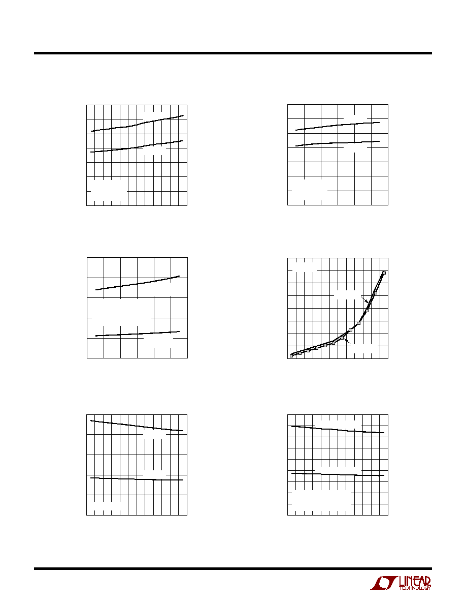
TYPICAL PERFOR
M
A
N
CE CHARACTERISTICS
U
W
Propagation Delay
vs Temperature
TEMPERATURE (
°
C)
14
12
10
8
6
4
2
0
PROPAGATION DELAY (ns)
1688/89 G01
0
20
40
60
80
100
V
DI
= 0V TO 3V
R
DIFF
= 50
C
L
= 25pF
V
DD
= 3V
V
DD
= 5V
Supply Current vs Data Rate
DATA RATE (Mbps)
250
200
150
100
50
0
SUPPLY CURRENT (mA)
1688/89 G03
0
20
40
60
80
100
120
V
DD
= 5V
R
DIFF
= 50
, PER DRIVER
C
L
= 25pF, PER DRIVER
T
A
= 25
°
C
4 DRIVERS
SWITCHING
1 DRIVER
SWITCHING
LOAD CAPACITANCE (pF)
14
12
10
8
6
4
2
0
PROPAGATION DELAY (ns)
1688/89 G02
0
10
20
30
40
50
60
V
DI
= 0V TO 3V
R
DIFF
= 50
T
A
= 25
°
C
V
DD
= 3V
V
DD
= 5V
Propagation Delay
vs Load Capacitance
TEMPERATURE (
°
C)
OUTPUT CURRENT (
µ
A)
1688/89 G04
4.0
3.5
3.0
2.5
2.0
1.5
1.0
0.5
0
0
20
40
60
80
100
V
DD
= 5V
V
OUT
= 12V
V
OUT
= 7V
TEMPERATURE (
°
C)
2.5
2.0
1.5
1.0
0.5
0
V
OD2
1688/89 G05
0
20
40
60
80
100
R
DIFF
= 50
V
DD
= 5V
V
DD
= 3V
TEMPERATURE (
°
C)
180
160
140
120
100
80
60
40
20
0
I
DD
(mA)
1688/89 G06
0
20
40
60
80
100
V
DD
= 5V
R
DIFF
= 50
, PER DRIVER
0.1Mbps
1 DRIVER LOADED
4 DRIVERS LOADED
Three-State Output Current
I
DD
vs Temperature
V
OD2
vs Temperature
5
LTC1688/LTC1689
PI
N
FU
N
CTIO
N
S
U
U
U
DI1 (Pin 1): Driver 1 Input. Do not float.
DO1A (Pin 2): Driver 1 Noninverting Output.
DO1B (Pin 3): Driver 1 Inverting Output.
EN (Pin 4, LTC1688): High True Enable Pin, enables all
four drivers. A low on Pin 4 and a high on Pin 12 will put
all driver outputs into a high impedance state. See
Function Tables for details. Do not float.
EN12 (Pin 4, LTC1689): Enables Drivers 1 and 2. A low on
Pin 4 will put the outputs of drivers 1 and 2 into a high
impedance state. See Function Tables for details. Do not
float.
DO2B (Pin 5): Driver 2 Inverting Output.
DO2A (Pin 6): Driver 2 Noninverting Output.
DI2 (Pin 7): Driver 2 Input. Do not float.
GND (Pin 8): Ground Connection. A good ground plane is
recommended for all applications.
DI3 (Pin 9): Driver 3 Input. Do not float.
DO3A (Pin 10): Driver 3 Noninverting Output.
DO3B (Pin 11): Driver 3 Inverting Output.
ENB (Pin 12, LTC1688): Low True Enable Pin, enables all
four drivers. A low on Pin 4 and a high on Pin 12 will put
all driver outputs into a high impedance state. See
Function Tables for details. Do not float.
EN34 (Pin 12, LTC1689): Enables Drivers 3 and 4. A low
on Pin 12 will put the outputs of drivers 3 and 4 into a high
impedance state. See Function Tables for details. Do not
float.
DO4B (Pin 13): Driver 4 Inverting Output.
DO4A (Pin 14): Driver 4 Noninverting Output.
DI4 (Pin 15): Driver 4 Input. Do not float.
V
DD
(Pin 16): Power Supply Input. This pin should be
bypassed with a 0.1
µ
F ceramic capacitor as close to the
pin as possible. Recommended: V
DD
= 3V to 5.25V.
FU CTIO TABLES
U
U
LTC1688
INPUTS
OUTPUTS
DI
EN
ENB
OUTA
OUTB
H
H
X
H
L
L
H
X
L
H
H
X
L
H
L
L
X
L
L
H
X
L
H
HI-Z
HI-Z
LTC1689
INPUTS
OUTPUTS
DI
EN12/EN34
OUTA
OUTB
H
H
H
L
L
H
L
H
X
L
HI-Z
HI-Z
1688/89 TC03
OUTPUT
UNDER TEST
C
L
S1
500
DD
V
S2
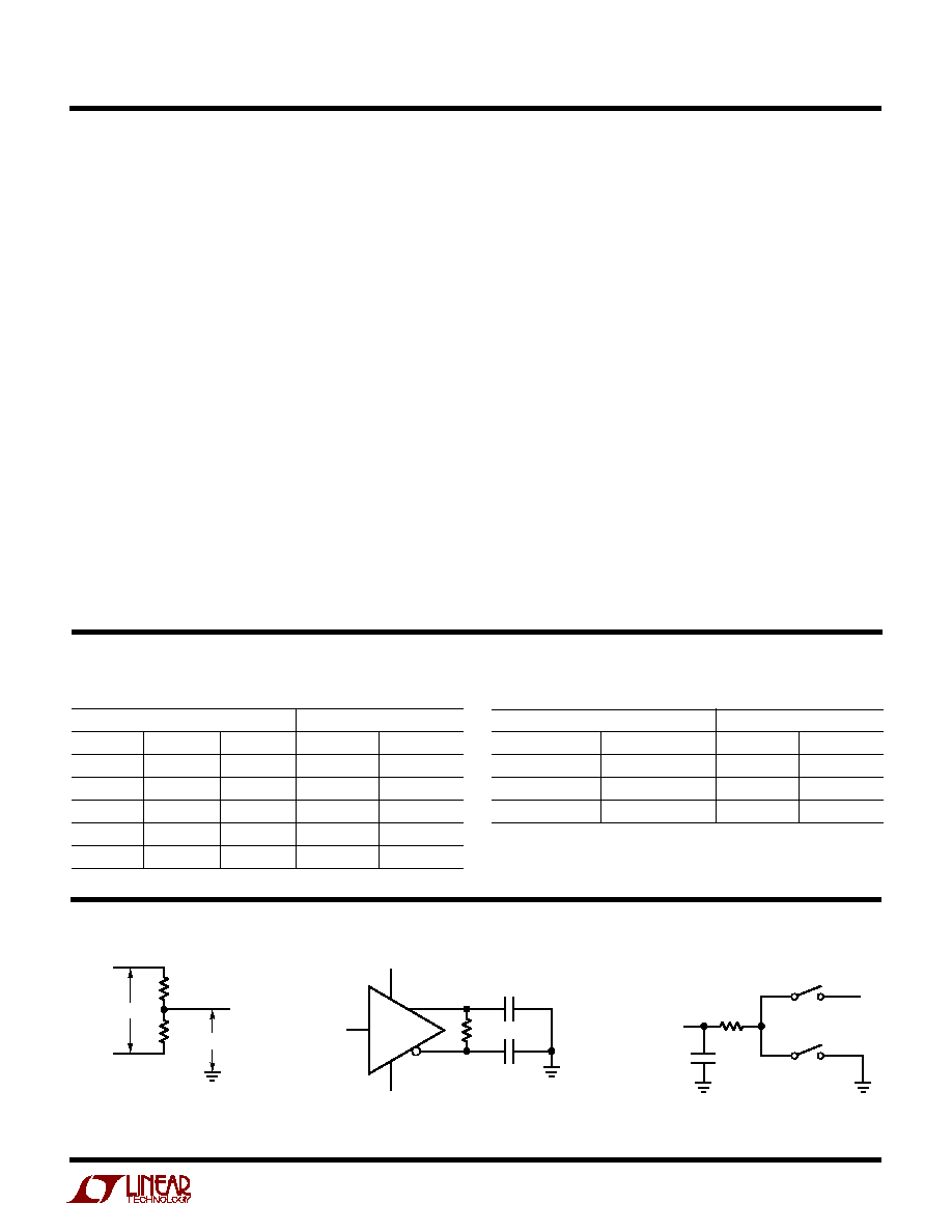
1688/89 TC01
A
B
R
R
OD
V
OC
V
Figure 1. Driver DC Test Load
Figure 3. Driver Timing Test Load
DRIVER
1688/89 TC02
ENB (EN34)
DI
A
B
EN (EN12)
R
DIFF
C
L1
C
L2
Figure 2. Driver Timing Test Circuit
TEST CIRCUITS