3727a1f.pm65
1
LTC3727A-1
3727a1f
Wide Output Voltage Range: 0.8V
V
OUT
14V
Out-of-Phase Controllers Reduce Required Input
Capacitance and Power Supply Induced Noise
OPTI-LOOP
®
Compensation Minimizes C
OUT
±1% Output Voltage Accuracy
Power Good Output Voltage Monitor
Phase-Lockable Fixed Frequency 250kHz to 550kHz
Dual N-Channel MOSFET Synchronous Drive
Wide V
IN
Range: 4V to 36V Operation
Very Low Dropout Operation: 99% Duty Cycle
Adjustable Soft-Start Current Ramping
Foldback Output Current Limiting
Output Overvoltage Protection
Low Shutdown I
Q
: 20
µA
Selectable Constant Frequency or Burst Mode
®
Operation
Small 28-Lead SSOP Package
The LTC
®
3727A-1 is a high performance dual step-down
switching regulator controller that drives all N-channel
synchronous power MOSFET stages. A constant fre-
quency current mode architecture allows phase-lockable
frequency of up to 550kHz. Power loss and noise due to
the ESR of the input capacitors are minimized by operating
the two controller output stages out of phase.
The LTC3727A-1 is an improved version of the LTC3727
family of parts. It has smaller output ripple while in the
drop-out condition and shorter minimum on-time.
OPTI-LOOP compensation allows the transient response
to be optimized over a wide range of output capacitance and
ESR values. There is a precision 0.8V reference and a power
good output indicator. A wide 4V to 30V (36V maximum)
input supply range encompasses all battery chemistries.
A RUN/SS pin for each controller provides soft-start.
Current foldback limits MOSFET heat dissipation during
short-circuit conditions. Output overvoltage protection
circuitry protects the controller until V
OUT
returns to
normal.
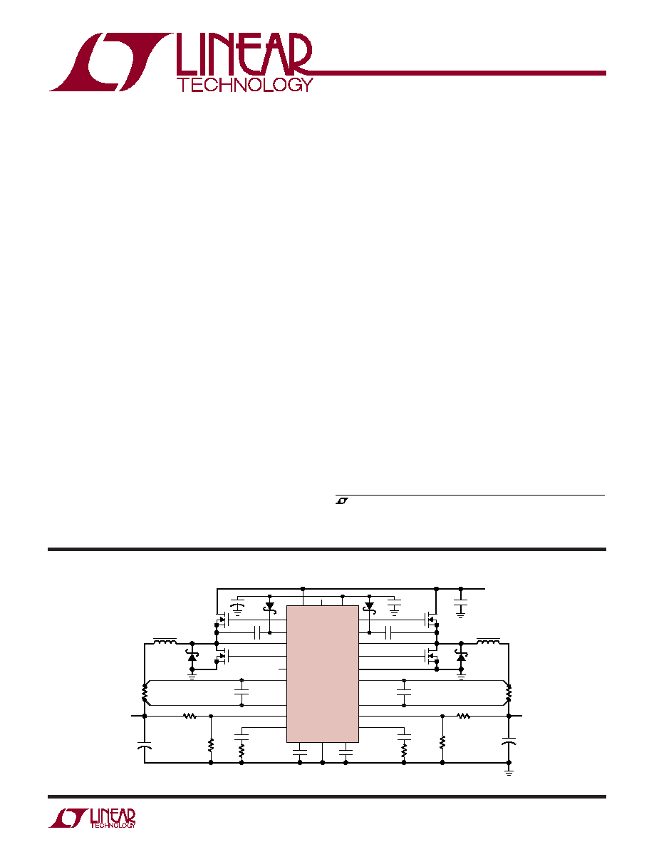
Telecom Systems
Automotive Systems
Battery-Operated Digital Devices
+
4.7
µF
M2
M1
0.1
µF
105k
1%
1000pF
8
µH
220pF
1
µF
CERAMIC
22
µF
50V
CERAMIC
+
47
µF
6V
SP
0.015
20k
1%
15k
V
OUT1
5V
5A
M4
M3
0.1
µF
280k
1%
15
µH
220pF
1000pF
+
56
µF
15V
SP
0.015
20k
1%
15k
V
OUT2
12V
4A
TG1
TG2
BOOST1
BOOST2
SW1
SW2
BG1
BG2
SGND
PGND
SENSE1
+
SENSE2
+
SENSE1
SENSE2
V
OSENSE1
V
OSENSE2
I
TH1
I
TH2
V
IN
PGOOD INTV
CC
RUN/SS1
RUN/SS2
V
IN
18V TO 28V
M1, M2, M3, M4: FDS6680A
3727 F01
0.1
µF
0.1
µF
LTC3727A-1
PLLIN
DESCRIPTIO
U
FEATURES
APPLICATIO S
U
TYPICAL APPLICATIO
U
, LTC and LT are registered trademarks of Linear Technology Corporation.
Burst Mode and OPTI-LOOP are registered trademarks of Linear Technology Corporation.
All other trademarks are the property of their respective owners.
Protected by U.S. Patents, including 5481178, 5929620, 6177787, 6144194, 6100678,
5408150, 6580258, 6304066, 5705919.
High Efficiency, 2-Phase
Synchronous Step-Down
Switching Regulators
Figure 1. High Efficiency Dual 12V/5V Step-Down Converter
2
LTC3727A-1
3727a1f
Input Supply Voltage (V
IN
) .........................36V to 0.3V
Top Side Driver Voltages
(BOOST1, BOOST2) ...................................42V to 0.3V
Switch Voltage (SW1, SW2) .........................36V to 5V
INTV
CC,
EXTV
CC
, (BOOST1-SW1),
(BOOST2-SW2) ........................................8.5V to 0.3V
RUN/SS1, RUN/SS2, PGOOD ..................... 7V to 0.3V
SENSE1
+
, SENSE2
+
, SENSE1
,
SENSE2
Voltages .....................................14V to 0.3V
PLLIN, PLLFLTR, FCB Voltages ........... INTV
CC
to 0.3V
I
TH1,
I
TH2
, V
OSENSE1
, V
OSENSE2
Voltages ... 2.7V to 0.3V
Peak Output Current <10
µs (TG1, TG2, BG1, BG2) ... 3A
INTV
CC
Peak Output Current ................................ 50mA
Operating Temperature Range (Note 2) .. 40
°C to 85°C
Junction Temperature (Note 3) ............................. 125
°C
Storage Temperature Range ................. 65
°C to 150°C
Lead Temperature (Soldering, 10 sec).................. 300
°C
T
JMAX
= 125
°C,
JA
= 95
°C/W
ABSOLUTE AXI U RATI GS
W
W
W
U
PACKAGE/ORDER I FOR ATIO
U
U
W
1
2
3
4
5
6
7
8
9
10
11
12
13
14
TOP VIEW
G PACKAGE
28-LEAD PLASTIC SSOP
28
27
26
25
24
23
22
21
20
19
18
17
16
15
RUN/SS1
SENSE1
+
SENSE1
V
OSENSE1
PLLFLTR
PLLIN
FCB
I
TH1
SGND
3.3V
OUT
I
TH2
V
OSENSE2
SENSE2
SENSE2
+
PGOOD
TG1
SW1
BOOST1
V
IN
BG1
EXTV
CC
INTV
CC
PGND
BG2
BOOST2
SW2
TG2
RUN/SS2
(Note 1)
The
denotes the specifications which apply over the full operating
temperature range, otherwise specifications are at T
A
= 25
°C. V
IN
= 15V, V
RUN/SS1, 2
= 5V unless otherwise noted.
ELECTRICAL CHARACTERISTICS
SYMBOL
PARAMETER
CONDITIONS
MIN
TYP
MAX
UNITS
Main Control Loops
V
OSENSE1, 2
Regulated Feedback Voltage
(Note 4); I
TH1, 2
Voltage = 1.2V
0.792
0.800
0.808
V
I
VOSENSE1, 2
Feedback Current
(Note 4)
5
50
nA
V
REFLNREG
Reference Voltage Line Regulation
V
IN
= 3.6V to 30V (Note 4)
0.002
0.02
%/V
V
LOADREG
Output Voltage Load Regulation
(Note 4)
Measured in Servo Loop;
I
TH
Voltage = 1.2V to 0.7V
0.1
0.5
%
Measured in Servo Loop;
I
TH
Voltage = 1.2V to 2.0V
0.1
0.5
%
g
m1, 2
Transconductance Amplifier g
m
I
TH1, 2
= 1.2V; Sink/Source 5
µA (Note 4)
1.3
mmho
g
mGBW1, 2
Transconductance Amplifier GBW
I
TH1, 2
= 1.2V (Note 4)
3
MHz
I
Q
Input DC Supply Current
(Note 5)
Normal Mode
V
IN
= 15V, EXTV
CC
Tied to V
OUT1
, V
OUT1
= 8.5V
670
µA
Shutdown
V
RUN/SS1, 2
= 0V
20
35
µA
ORDER PART NUMBER
Consult LTC Marketing for parts specified with wider operating temperature ranges.
Order Options Tape and Reel: Add #TR
Lead Free: Add #PBF Lead Free Tape and Reel: Add #TRPBF
Lead Free Part Marking:
http://www.linear.com/leadfree/
LTC3727AEG-1
3
LTC3727A-1
3727a1f
The
denotes the specifications which apply over the full operating
temperature range, otherwise specifications are at T
A
= 25
°C. V
IN
= 15V, V
RUN/SS1, 2
= 5V unless otherwise noted.
ELECTRICAL CHARACTERISTICS
SYMBOL
PARAMETER
CONDITIONS
MIN
TYP
MAX
UNITS
V
FCB
Forced Continuous Threshold
0.76
0.800
0.84
V
I
FCB
Forced Continuous Pin Current
V
FCB
= 0.85V
0.30
0.18
0.05
µA
V
BINHIBIT
Burst Inhibit (Constant Frequency)
Measured at FCB pin
6.8
7.3
V
Threshold
UVLO
Undervoltage Lockout
V
IN
Ramping Down
3.5
4
V
V
OVL
Feedback Overvoltage Lockout
Measured at V
OSENSE1, 2
0.84
0.86
0.88
V
I
SENSE
Sense Pins Total Source Current
(Each Channel) V
SENSE1
, 2
= V
SENSE1
+
, 2
+
= 0V
85
60
µA
DF
MAX
Maximum Duty Factor
In Dropout
98
99.4
%
I
RUN/SS1, 2
Soft-Start Charge Current
V
RUN/SS1, 2
= 1.9V
0.5
1.2
µA
V
RUN/SS1, 2
ON RUN/SS Pin ON Threshold
V
RUN/SS1,
V
RUN/SS2
Rising
1.0
1.5
1.9
V
V
SENSE(MAX)
Maximum Current Sense Threshold
V
OSENSE1, 2
= 0.7V,V
SENSE1, 2
= 12V
105
135
165
mV
TG Transition Time:
(Note 6)
TG1, 2 t
r
Rise Time
C
LOAD
= 3300pF
50
90
ns
TG1, 2 t
f
Fall Time
C
LOAD
= 3300pF
50
90
ns
BG Transition Time:
(Note 6)
BG1, 2 t
r
Rise Time
C
LOAD
= 3300pF
40
90
ns
BG1, 2 t
f
Fall Time
C
LOAD
= 3300pF
40
80
ns
TG/BG t
1D
Top Gate Off to Bottom Gate On Delay
C
LOAD
= 3300pF Each Driver
90
ns
Synchronous Switch-On Delay Time
BG/TG t
2D
Bottom Gate Off to Top Gate On Delay
C
LOAD
= 3300pF Each Driver
90
ns
Top Switch-On Delay Time
t
ON(MIN)
Minimum On-Time
Tested with a Square Wave (Note 7)
120
ns
INTV
CC
Linear Regulator
V
INTVCC
Internal V
CC
Voltage
8.5V < V
IN
< 30V, V
EXTVCC
= 6V
7.2
7.5
7.8
V
V
LDO
INT
INTV
CC
Load Regulation
I
CC
= 0mA to 20mA, V
EXTVCC
= 6V
0.2
1.0
%
V
LDO
EXT
EXTV
CC
Voltage Drop
I
CC
= 20mA, V
EXTVCC
= 8.5V
70
160
mV
V
EXTVCC
EXTV
CC
Switchover Voltage
I
CC
= 20mA, EXTV
CC
Ramping Positive
6.9
7.3
V
V
LDOHYS
EXTV
CC
Hysteresis
0.3
V
Oscillator and Phase-Locked Loop
f
NOM
Nominal Frequency
V
PLLFLTR
= 1.2V
350
380
430
kHz
f
LOW
Lowest Frequency
V
PLLFLTR
= 0V
220
255
290
kHz
f
HIGH
Highest Frequency
V
PLLFLTR
2.4V
460
530
580
kHz
R
PLLIN
PLLIN Input Resistance
100
k
I
PLLFLTR
Phase Detector Output Current
Sinking Capability
f
PLLIN
< f
OSC
15
µA
Sourcing Capability
f
PLLIN
> f
OSC
15
µA
4
LTC3727A-1
3727a1f
Note 1: Stresses beyond those listed under Absolute Maximum Ratings
may cause permanent damage to the device. Exposure to any Absolute
Maximum Rating condition for extended periods may affect device
reliability and lifetime.
Note 2: The LTC3727AE-1 is guaranteed to meet performance
specifications from 0
°C to 85°C. Specifications over the 40°C to 85°C
operating temperature range are assured by design, characterization and
correlation with statistical process controls.
Note 3: T
J
is calculated from the ambient temperature T
A
and power
dissipation P
D
according to the following formulas:
LTC3727AEG-1: T
J
= T
A
+ (P
D
· 95
°C/W)
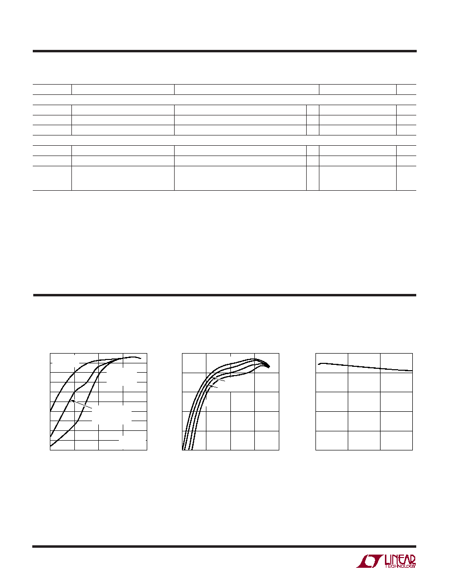
Efficiency vs Output Current
and Mode (Figure 13)
Efficiency vs Output Current
(Figure 13)
Efficiency vs Input Voltage
(Figure 13)
TYPICAL PERFOR A CE CHARACTERISTICS
U
W
OUTPUT CURRENT (A)
0.001
0
EFFICIENCY (%)
10
30
40
50
100
70
0.01
0.1
1
3727 G01
20
80
90
60
10
FORCED
CONTINUOUS
MODE
Burst Mode
OPERATION
V
IN
= 15V
V
OUT
= 8.5V
CONSTANT
FREQUENCY
(BURST DISABLE)
OUTPUT CURRENT (A)
0.001
EFFICIENCY (%)
70
80
10
3727 G02
60
50
0.01
0.1
1
100
90
V
IN
= 10V
V
IN
= 15V
V
IN
= 7V
V
IN
= 20V
V
OUT
= 5V
INPUT VOLTAGE (V)
5
EFFICIENCY (%)
70
80
3727 G03
60
50
15
25
35
100
V
OUT
= 5V
I
OUT
= 3A
90
The
denotes the specifications which apply over the full operating
temperature range, otherwise specifications are at T
A
= 25
°C. V
IN
= 15V, V
RUN/SS1, 2
= 5V unless otherwise noted.
ELECTRICAL CHARACTERISTICS
Note 4: The LTC3727A-1 is tested in a feedback loop that servos V
ITH1, 2
to a specified voltage and measures the resultant V
OSENSE1, 2.
Note 5: Dynamic supply current is higher due to the gate charge being
delivered at the switching frequency. See Applications Information.
Note 6: Rise and fall times are measured using 10% and 90% levels. Delay
times are measured using 50% levels.
Note 7: The minimum on-time condition is specified for an inductor
peak-to-peak ripple current
40% of I
MAX
(see minimum on-time
considerations in the Applications Information section).
SYMBOL
PARAMETER
CONDITIONS
MIN
TYP
MAX
UNITS
3.3V Linear Regulator
V
3.3OUT
3.3V Regulator Output Voltage
No Load
3.25
3.35
3.45
V
V
3.3IL
3.3V Regulator Load Regulation
I
3.3
= 0mA to 10mA
0.5
2.5
%
V
3.3VL
3.3V Regulator Line Regulation
6V < V
IN
< 30V
0.05
0.3
%
PGOOD Output
V
PGL
PGOOD Voltage Low
I
PGOOD
= 2mA
0.1
0.3
V
I
PGOOD
PGOOD Leakage Current
V
PGOOD
= 5V
±1
µA
V
PG
PGOOD Trip Level, Either Controller
V
OSENSE
with Respect to Set Output Voltage
V
OSENSE
Ramping Negative
6
7.5
9.5
%
V
OSENSE
Ramping Positive
6
7.5
9.5
%
5
LTC3727A-1
3727a1f
Maximum Current Sense Threshold
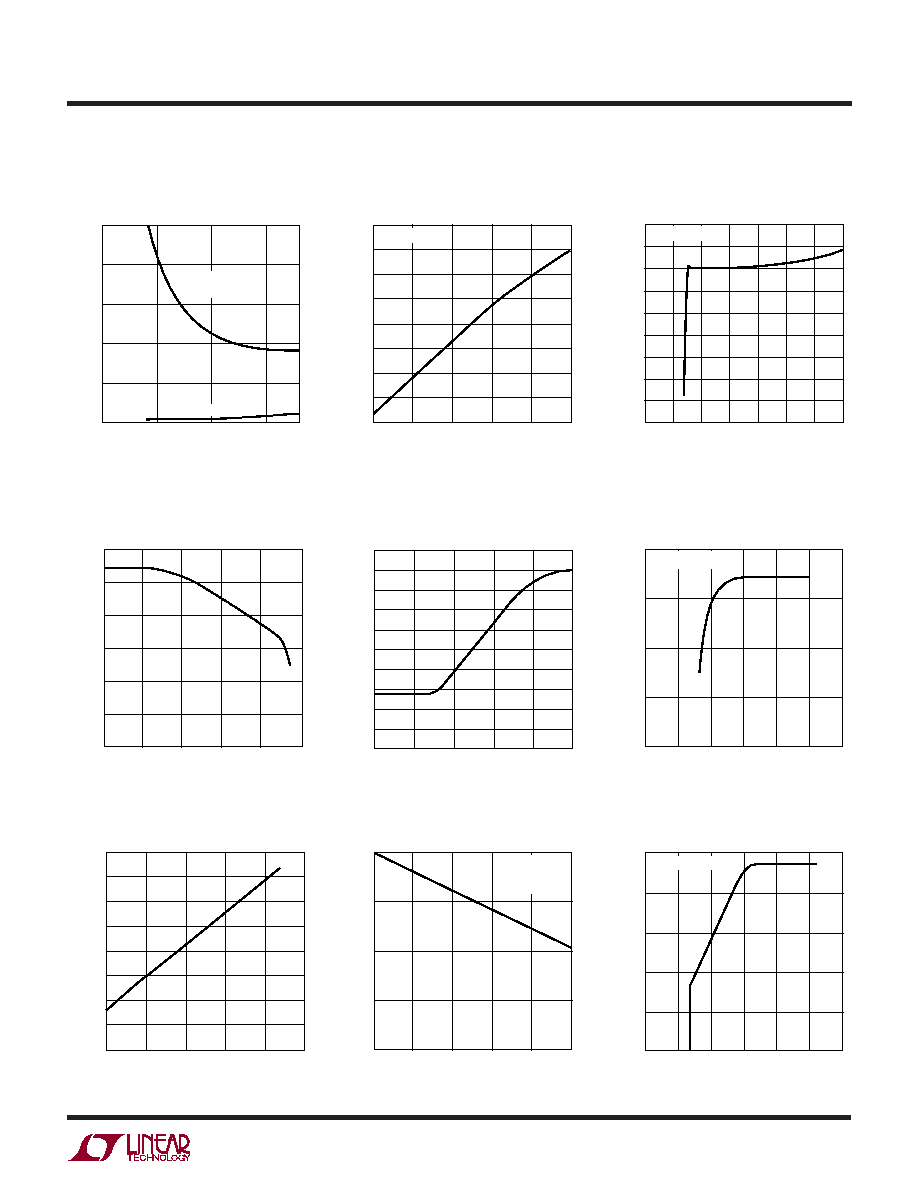
vs Duty Factor
Maximum Current Sense Threshold
vs Percent of Nominal Output
Voltage (Foldback)
Maximum Current Sense Threshold
vs V
RUN/SS
(Soft-Start)
Current Sense Threshold
vs I
TH
Voltage
Load Regulation
V
ITH
vs V
RUN/SS
TYPICAL PERFOR A CE CHARACTERISTICS
U
W
DUTY FACTOR (%)
0
0
V
SENSE
(mV)
25
50
75
100
125
150
20
40
60
80
3727 G07
100
PERCENT OF NOMINAL OUTPUT VOLTAGE (%)
0
V
SENSE
(mV)
90
120
150
80
3727 G08
60
30
75
105
135
45
15
0
20
40
60
100
V
RUN/SS
(V)
0
50
V
SENSE
(mV)
75
100
125
150
1
2
3
4
3727 G09
5
6
V
SENSE(CM)
= 1.6V
V
ITH
(V)
0
V
SENSE
(mV)
25
50
75
1.5
2.5
3727 G10
0
25
50
0.5
1.0
2.0
100
125
150
LOAD CURRENT (A)
0
NORMALIZED V
OUT
(%)
0.2
0.1
4
3727 G11
0.3
0.4
1
2
3
5
0.0
FCB = 0V
V
IN
= 15V
FIGURE 1
V
RUN/SS
(V)
0
0
V
ITH
(V)
0.5
1.0
1.5
2.0
2.5
1
2
3
4
3727 G12
5
6
V
OSENSE
= 0.7V
Supply Current vs Input Voltage
and Mode (Figure 13)
EXTV
CC
Voltage Drop
INPUT VOLTAGE (V)
0
0
SUPPLY CURRENT (
µ
A)
400
1000
10
20
3727 G04
200
800
600
30
BOTH
CONTROLLERS ON
SHUTDOWN
CURRENT (mA)
0
EXTV
CC
VOLTAGE DROP (mV)
60
80
100
30
50
3727 G05
40
20
0
10
20
40
120
140
160
V
EXTVCC
= 8.5V
Internal 7.5V LDO Line Regulation
INPUT VOLTAGE (V)
0
6.8
INTV
CC
VOLTAGE (V)
6.9
7.1
7.2
7.3
20
7.7
3727 G06
7.0
10
5
25
30
15
35
7.4
7.5
7.6
I
LOAD
= 1mA