4011f.pm6
1
LTC4011
4011f
, LTC and LT are registered trademarks of Linear Technology Corporation. PowerPath is
a trademark of Linear Technology Corporation. All other trademarks are the property of
their respective owners.
High Efficiency Standalone
Nickel Battery Charger
Complete NiMH/NiCd Charger for 1 to 16 Cells
No Microcontroller or Firmware Required
550kHz Synchronous PWM Current Source Controller
No Audible Noise with Ceramic Capacitors
PowerPath
TM
Control Support
Programmable Charge Current: 5% Accuracy
Wide Input Voltage Range: 4.5V to 34V
Automatic Trickle Precharge
V Fast Charge Termination
Optional
T/t Fast Charge Termination
Automatic NiMH Top-Off Charge
Programmable Timer
Automatic Recharge
Multiple Status Outputs
Micropower Shutdown
20-Lead Thermally Enhanced TSSOP Package
Integrated or Standalone Battery Charger
Portable Instruments or Consumer Products
Battery-Powered Diagnostics and Control
Back-Up Battery Management
The LTC
®
4011 provides a complete, cost-effective nickel
battery fast charge solution in a small package using few
external components. A 550kHz PWM current source
controller and all necessary charge initiation, monitoring
and termination control circuitry are included.
The LTC4011 automatically senses the presence of a DC
adapter and battery insertion or removal. Heavily dis-
charged batteries are precharged with a trickle current.
The LTC4011 can simultaneously use both
V and T/t
fast charge termination techniques and can detect various
battery faults. If necessary, a top-off charge is automati-
cally applied to NiMH batteries after fast charging is
completed. The IC will also resume charging if the battery
self-discharges after a full charge cycle.
All LTC4011 charging operations are qualified by actual
charge time and maximum average cell voltage. Charging
may also be gated by minimum and maximum tempera-
ture limits. NiMH or NiCd fast charge termination param-
eters are pin-selectable.
Integrated PowerPath control support ensures that the
system remains powered at all times without allowing load
transients to adversely affect charge termination.
FEATURES
DESCRIPTIO
U
APPLICATIO S
U
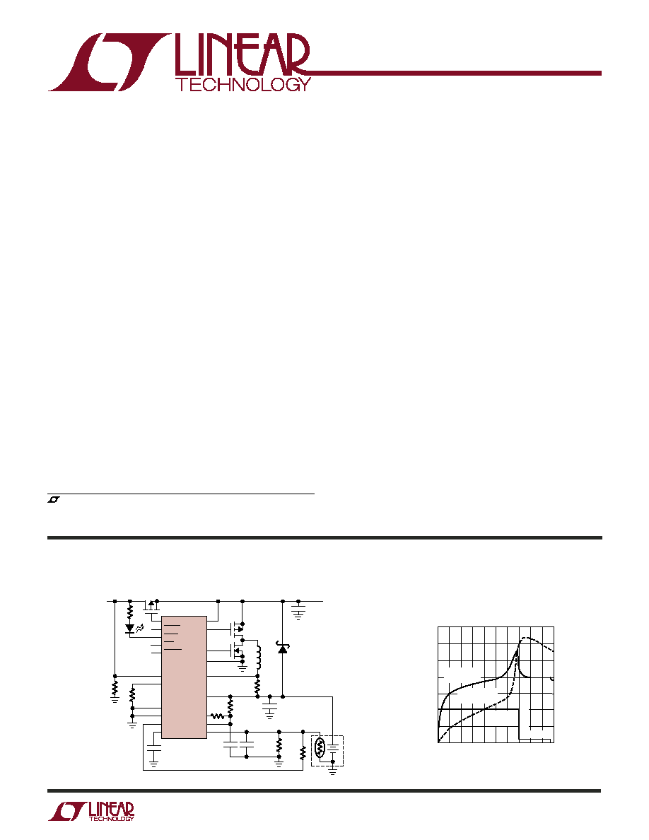
TYPICAL APPLICATIO
U
INFET
FAULT
CHRG
TOC
READY
V
CC
TGATE
V
CDIV
V
CELL
V
TEMP
LTC4011
DCIN
TIMER
GND
CHEM
V
RT
INTV
DD
SENSE
BAT
FROM
ADAPTER
4.5V TO 34V
10
µH
10
µF
TO
SYSTEM
LOAD
0.05
2-CELL
NiMH PACK
WITH 10k NTC
(2Ahr)
4011 TA01a
3k
20k
49.9k
10k
10k
9.76k
0.1
µF
0.033
µF
0.068
µF
10
µF
28k
BGATE
PGND
2A NiMH Battery Charger
TIME (MINUTES)
0
1.25
CELL VOLTAGE (V)
BATTERY TEMPERATURE (
°
C)
1.30
1.40
1.45
1.50
1.60
4011 TA01b
1.35
1.55
28
30
34
36
38
42
32
40
40
100
20
60
80
SINGLE CELL
VOLTAGE
CHARGE
CURRRENT
BATTERY
TEMPERATURE
2A
1A
TOP OFF
2A NiMH Charge Cycle at 1C
2
LTC4011
4011f
ORDER PART
NUMBER
(Note 1)
V
CC
(Input Supply) to GND ....................... 0.3V to 36V
DCIN to GND ............................................ 0.3V to 36V
FAULT, CHRG, V
CELL
, V
CDIV
, SENSE, BAT, TOC
or READY to GND .......................... 0.3V to V
CC
+ 0.3V
SENSE to BAT ......................................................
±0.3V
CHEM, V
TEMP
or TIMER to GND .............. 0.3V to 3.5V
PGND to GND ......................................................
±0.3V
Operating Ambient Temperature Range
(Note 2) ....................................................... 0
°C to 85°C
Operating Junction Temperature (Note 3) ........... 125
°C
Storage Temperature Range ................. 65
°C to 150°C
Lead Temperature (Soldering, 10 sec).................. 300
°C
LTC4011CFE
T
JMAX
= 125
°C,
JA
= 38
°C/W
EXPOSED PAD (PIN 21) IS GND. MUST BE SOLDERED TO
PCB TO OBTAIN SPECIFIED THERMAL RESISTANCE
ABSOLUTE
M
AXI
M
U
M
RATINGS
W
W
W
U
PACKAGE/ORDER I
N
FOR
M
ATIO
N
W
U
U
Consult LTC Marketing for parts specified with wider operating temperature ranges.
FE PACKAGE
20-LEAD PLASTIC TSSOP
1
2
3
4
5
6
7
8
9
10
TOP VIEW
20
19
18
17
16
15
14
13
12
11
DCIN
FAULT
CHRG
CHEM
GND
V
RT
V
TEMP
V
CELL
V
CDIV
TIMER
INFET
READY
V
CC
TGATE
PGND
BGATE
INTV
DD
TOC
BAT
SENSE
21
The
indicates specifications which apply over the full operating
temperature range, otherwise specifications are at T
A
= 25
°C. V
CC
= 12V, BAT = 4.8V, GND = PGND = 0V, unless otherwise noted.
ELECTRICAL CHARACTERISTICS
SYMBOL
PARAMETER
CONDITIONS
MIN
TYP
MAX
UNITS
V
CC
Supply
V
CC
Input Voltage Range
4.5
34
V
I
SHDN
Shutdown Quiescent Current (Note 5)
V
CC
= BAT = 4.8V
5
10
µA
I
Q
Quiescent Current
Waiting to Charge (Pause)
3
5
mA
I
CC
Operating Current
Fast Charge State, No Gate Load
5
9
mA
V
UVLO
Undervoltage Threshold Voltage
V
CC
Increasing
3.85
4.2
4.45
V
V
UV(HYST)
Undervoltage Hysteresis Voltage
170
mV
V
SHDNI
Shutdown Threshold Voltage
DCIN V
CC
, DCIN Increasing
15
30
50
mV
V
SHDND
Shutdown Threshold Voltage
DCIN V
CC
, DCIN Decreasing
60
25
5
mV
V
CE
Charge Enable Threshold Voltage
V
CC
BAT, V
CC
Increasing
400
510
600
mV
INTV
DD
Regulator
V
DD
Output Voltage
No Load
4.5
5
5.5
V
I
DD
Short-Circuit Current (Note 6)
INTV
DD
= 0V
100
50
10
mA
INTV
DD(MIN)
Output Voltage
V
CC
= 4.5V, I
DD
= 10mA
3.85
V
Thermistor Termination
V
RT
Output Voltage
R
L
= 10k
3.125
3.3
3.475
V
3.05
3.55
V
I
RT
Short-Circuit Current
V
RT
= 0V
9
1
mA
Order Options Tape and Reel: Add #TR
Lead Free: Add #PBF Lead Free Tape and Reel: Add #TRPBF
Lead Free Part Marking:
http://www.linear.com/leadfree/
3
LTC4011
4011f
The
indicates specifications which apply over the full operating
temperature range, otherwise specifications are at T
A
= 25
°C. V
CC
= 12V, BAT = 4.8V, GND = PGND = 0V, unless otherwise noted.
ELECTRICAL CHARACTERISTICS
SYMBOL
PARAMETER
CONDITIONS
MIN
TYP
MAX
UNITS
PWM Current Source
V
FS
BAT SENSE Full-Scale Regulation
0.3V < BAT < V
CC
0.3V (Note 5)
95
100
105
mV
Voltage (Fast Charge)
BAT = 4.8V
95
100
105
mV
V
PC
BAT SENSE Precharge Regulation
0.3V < BAT < V
CC
0.3V (Note 5)
16
20
24
mV
Voltage
BAT = 4.8V
16
20
24
mV
V
TC
BAT SENSE Top-Off Charge
0.3V < BAT < V
CC
0.3V (Note 5)
6.5
10
13.5
mV
Regulation Voltage
BAT = 4.8V
6.5
10
13.5
mV
V
LI
BAT SENSE Line Regulation
5.5V < V
CC
< 25V, Fast Charge
±0.3
mV
I
BAT
BAT Input Bias Current
0.3V < BAT < V
CC
0.1V
2
2
mA
I
SENSE
SENSE Input Bias Current
SENSE = BAT
50
150
µA
I
OFF
Input Bias Current
SENSE or BAT, V
CELL
= 0V
1
0
1
µA
f
TYP
Typical Switching Frequency
460
550
615
kHz
f
MIN
Minimum Switching Frequency
20
30
kHz
DC
MAX
Maximum Duty Cycle
98
99
%
V
OL(TG)
TGATE Output Voltage Low
V
CC
> 9V, No Load
5
5.6
8.75
V
(V
CC
TGATE, Note 7)
V
CC
< 7.5V, No Load
V
CC
V
CC
V
0.5
V
OH(TG)
TGATE Output Voltage High
V
CC
TGATE, No Load
0
50
mV
t
R(TG)
TGATE Rise Time
C
LOAD
= 3nF, 10% to 90%
35
100
ns
t
F(TG)
TGATE Fall Time
C
LOAD
= 3nF, 10% to 90%
45
100
ns
V
OL(BG)
BGATE Output Voltage Low
No Load
0
50
mV
V
OH(BG)
BGATE Output Voltage High
No Load
INTV
DD
INTV
DD
V
0.075
t
R(BG)
BGATE Rise Time
C
LOAD
= 1.6nF, 10% to 90%
35
65
ns
t
F(BG)
BGATE Fall Time
C
LOAD
= 1.6nF, 10% to 90%
15
65
ns
ADC Inputs
I
LEAK
Analog Channel Leakage
0V < V
CELL
< 2V, 550mV < V
TEMP
< 2V
±100
nA
Charger Thresholds
V
BP
Battery Present Threshold Voltage
320
350
370
mV
V
BOV
Battery Overvoltage
1.85
1.95
2.05
V
V
MFC
Minimum Fast Charge Voltage
850
900
950
mV
V
FCBF
Fast Charge Battery Fault Voltage
1.17
1.22
1.27
V
V
TERM
V Termination
CHEM = 3.3V (NiCd)
16
20
25
mV
CHEM = 0V (NiMH)
6
10
14
mV
V
AR
Automatic Recharge Voltage
V
CELL
Decreasing
1.275
1.325
1.375
V
T
TERM
T Termination (Note 8)
CHEM = 3.3V (NiCd)
1.3
2
2.7
°C/min
CHEM = 0V (NiMH)
0.5
1
1.5
°C/min
T
MIN
Minimum Charging Temperature
V
TEMP
Increasing
0
5
9
°C
(Note 8)
T
MAXI
Maximum Charge Initiation
V
TEMP
Decreasing, Not Charging
41.5
45
47
°C
Temperature (Note 8)
T
MAXC
Maximum Fast Charge Temperature
V
TEMP
Decreasing, Fast Charge
57
60
63
°C
(Note 8)
V
TEMP(D)
V
TEMP
Disable Threshold Voltage
2.8
3.3
V
V
TEMP(P)
Pause Threshold Voltage
130
280
mV
4
LTC4011
4011f
The
indicates specifications which apply over the full operating
temperature range, otherwise specifications are at T
A
= 25
°C. V
CC
= 12V, BAT = 4.8V, GND = PGND = 0V, unless otherwise noted.
ELECTRICAL CHARACTERISTICS
Note 1: Absolute Maximum Ratings are those values beyond which the life
of the device may be impaired.
Note 2: The LTC4011C is guaranteed to meet performance specifications
from 0
°C to 70°C. Specifications over the 0°C to 85°C operating
temperature range are assured by design, characterization and correlation
with statistical process controls.
Note 3: Operating junction temperature T
J
(in
°C) is calculated from the
ambient temperature T
A
and the total continuous package power
dissipation P
D
(in watts) by the formula:
T
J
= T
A
+
JA
· P
D
Refer to the Applications Information section for details. This IC includes
overtemperature protection that is intended to protect the device during
momentary overload conditions. Junction temperature will exceed 125
°C
when overtemperature protection is active. Continuous operation above
the specified maximum operating junction temperature may result in
device degradation or failure.
Note 4: All current into device pins is positive. All current out of device
pins is negative. All voltages are referenced to GND, unless otherwise
specified.
Note 5: These limits are guaranteed by correlation to wafer level
measurements.
Note 6: Output current may be limited by internal power dissipation. Refer
to the Applications Information section for details.
Note 7: Either TGATE V
OH
may apply for 7.5V < V
CC
< 9V.
Note 8: These limits apply specifically to the thermistor network shown in
Figure 5 in the Applications Information section with the values specified
for a 10k NTC (
of 3750). Limits are then guaranteed by specific V
TEMP
voltage measurements during test.
SYMBOL
PARAMETER
CONDITIONS
MIN
TYP
MAX
UNITS
Charger Timing
t
TIMER
Internal Time Base Error
10
10
%
t
MAX
Programmable Timer Error
R
TIMER
= 49.9k
20
20
%
PowerPath Control
V
FR
INFET Forward Regulation Voltage
DCIN V
CC
30
55
100
mV
V
OL(INFET)
Output Voltage Low
V
CC
INFET, No Load
3.75
5.2
7
V
V
OH(INFET)
Output Voltage High
V
CC
INFET, No Load
0
50
mV
t
OFF(INFET)
INFET OFF Delay Time
C
LOAD
= 10nF, INFET to 50%
3
15
µs
Status and Chemistry Select
V
OL
Output Voltage Low (I
LOAD
= 10mA)
V
CDIV
435
700
mV
All Other Status Outputs
300
600
mV
I
LKG
Output Leakage Current
All Status Outputs Inactive, V
OUT
= V
CC
10
10
µA
I
IH(VCDIV)
Input Current High
V
CDIV
= V
BAT
(Shutdown)
1
1
µA
V
IL
Input Voltage Low
CHEM (NiMH)
900
mV
V
IH
Input Voltage High
CHEM (NiCd)
2.85
V
I
IL
Input Current Low
CHEM = GND
20
5
µA
I
IH
Input Current High
CHEM = 3.3V
20
20
µA
5
LTC4011
4011f
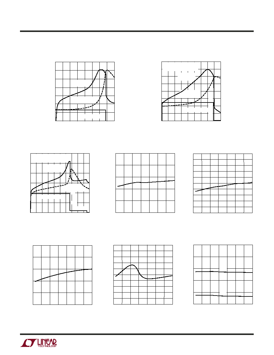
TYPICAL PERFOR A CE CHARACTERISTICS
U
W
NiCd Charge at 1C
NiCd Charge at 2C
NiMH Charge at 0.5C
TIME (MINUTES)
0
SINGLE CELL VOLTAGE (V)
BATTERY TEMPERATURE (
°
C)
1.50
1.55
1.60
60
4011 G01
1.45
1.40
20
40
80
1.35
1.30
1.65
30
32
34
28
26
24
1A
22
36
CHARGE CURRENT
BATTERY
TEMPERATURE
SINGLE CELL
VOLTAGE
TIME (MINUTES)
0
SINGLE CELL VOLTAGE (V)
BATTERY TEMPERATURE (
°
C)
1.60
1.65
1.70
30
4011 G02
1.55
1.50
10
20
40
1.45
1.35
1.40
1.75
40
45
50
35
30
25
15
20
55
CHARGE CURRENT
BATTERY
TEMPERATURE
SINGLE CELL
VOLTAGE
1A
2A
3A
4 SERIES NiCd 1300mAhr
SC CELLS CHARGED AT 2C
TIME (MINUTES)
1.30
SINGLE CELL VOLTAGE (V)
BATTERY TEMPEATURE (
°
C)
1.40
1.50
1.60
1.45
1.45
1.55
15
25
35
45
20
30
40
120
4011 G03
0
20 40
80 100
140 160
60
180 200
CHARGE CURRENT
TOP OFF
BATTERY
TEMPERATURE
SINGLE CELL
VOLTAGE
1A
0.5A
4 SERIES NiMH 2100mAhr
AA CELLS CHARGED AT 0.5C
TEMPERATURE (
°C)
50
30
320
VOLTAGE (mV)
340
370
10
30
50
4011 G04
330
360
350
10
70
90
TEMPERATURE (
°C)
50
850
VOLTAGE (mV)
860
880
890
900
950
920
10
30
50
4011 G05
870
930
940
910
30
10
70
90
Battery Present Threshold (per Cell)
Minimum Fast Charge Threshold
(per Cell)
Automatic Recharge Threshold
(per Cell)
Battery Overvoltage Threshold
(per Cell)
TEMPERATURE (
°C)
50
1.85
VOLTAGE (V)
1.87
1.91
1.93
1.95
2.05
1.99
10
30
50
4011 G07
1.89
2.01
2.03
1.97
30
10
70
90
V Termination (per Cell)
TEMPERATURE (
°C)
50
30
25
VOLTAGE (mV)
15
0
10
30
50
4011 G08
20
5
10
10
70
90
NiMH
NiCd
TEMPERATURE (
°C)
50
30
1.275
VOLTAGE (V) 1.315
1.375
10
30
50
4011 G06
1.295
1.355
1.335
10
70
90