The SY100EL14V is a low skew 1:5 clock distribution
chip designed explicitly for low skew clock distribution
applications. The device can be driven by either a
differential or single-ended ECL or, if positive power
supplies are used, PECL input signal. The EL14V is
suitable for operation in systems operating from 3.3V to
5.0V supplies. If a single-ended input is to be used the
V
BB
output should be connected to the CLK input and
bypassed to ground via a 0.01
µ
F capacitor. The V
BB
output is designed to act as the switching reference for
the input of the EL14V under single-ended input
conditions, as a result this pin can only source/sink up to
0.5mA of current.
The EL14V features a multiplexed clock input to allow
for the distribution of a lower speed scan or test clock
along with the high speed system clock. When LOW (or
left open and pulled LOW by the input pull-down resistor)
the SEL pin will select the differential clock input.
The common enable (EN) is synchronous so that the
outputs will only be enabled/disabled when they are
already in the LOW state. This avoids any chance of
generating a runt clock pulse when the device is enabled/
disabled as can happen with an asynchronous control.
The internal flip flop is clocked on the falling edge of the
input clock, therefore all associated specification limits
are referenced to the negative edge of the clock input.
When both differential inputs are left open, CLK input
will pull down to V
EE
and CLK input will bias around
V
CC
/2.
Pin
Function
CLK
Differential Clock Inputs
SCLK
Scan Clock Input
EN
Synchronous Enable
SEL
Clock Select Input
V
BB
Reference Output
Q
0-4
Differential Clock Outputs
TRUTH TABLE
PIN NAMES
FEATURES
DESCRIPTION
Rev.: A
Amendment: /0
Issue Date: October 1999
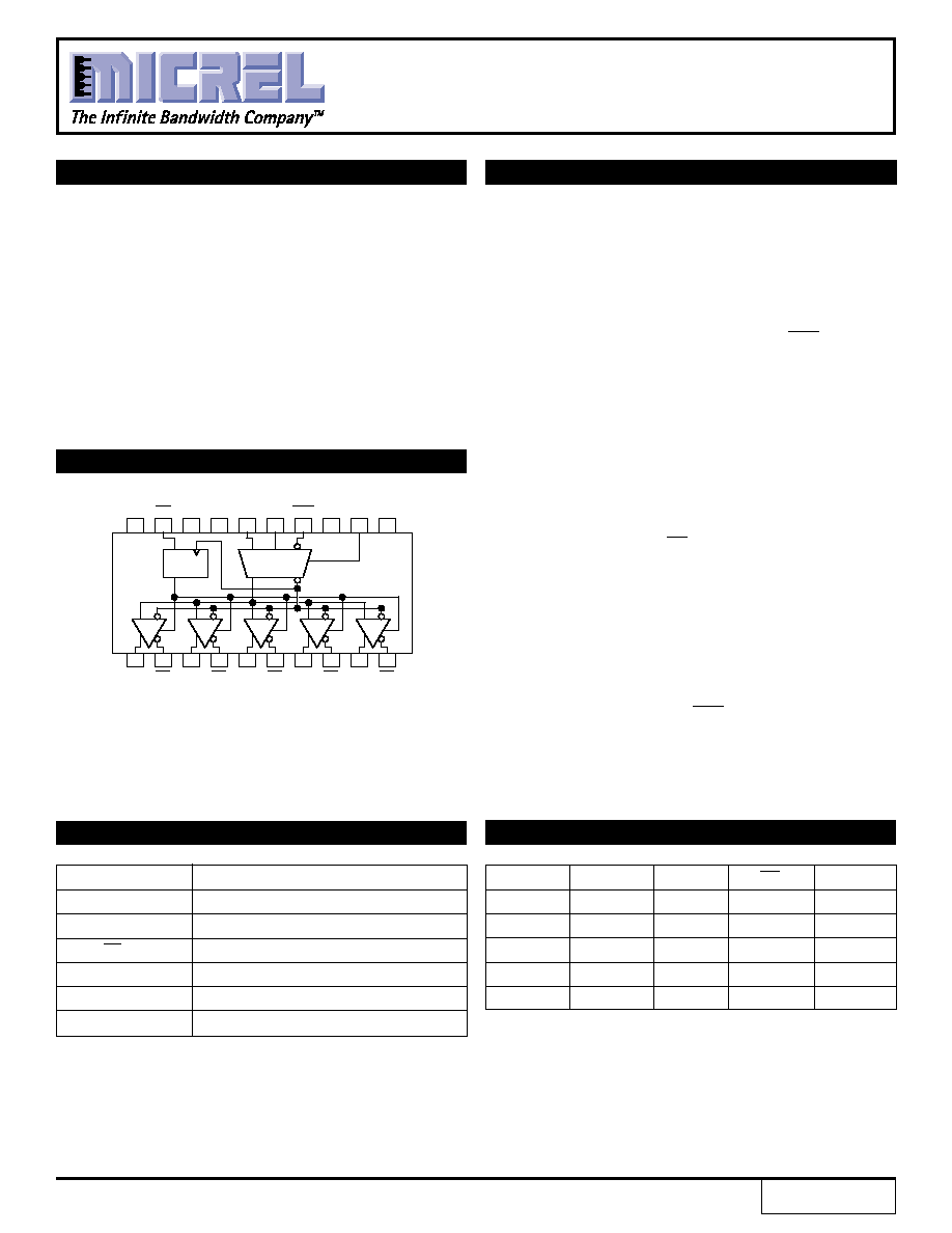
PIN CONFIGURATION/BLOCK DIAGRAM
ClockWorksTM
SY100EL14V
CLK
SCLK
SEL
EN
Q
L
X
L
L
L
H
X
L
L
H
X
L
H
L
L
X
H
H
L
H
X
X
X
H
L*
* On next negative transition of CLK or SCLK
1
Q0
Q0
Q1
Q1
Q2
Q2
Q3
Q3
Q4
Q4
20
V
CC
EN VCC NC SCLK CLK CLK V
BB
SEL V
EE
2
19
3
18
4
17
5
16
6
15
7
14
8
13
9
12
10
11
1
0
D
Q
SOIC
TOP VIEW
s
3.3V and 5V power supply options
s
Typical 30ps output-to-output skew
s
Max. 50ps output-to-output skew
s
Synchronous enable/disable
s
Multiplexed clock input
s
75K
internal input pull-down resistors
s
Available in 20-pin SOIC package
5V/3.3V 1:5 CLOCK
DISTRIBUTION
1
2
ClockWorksTM
SY100EL14V
Micrel
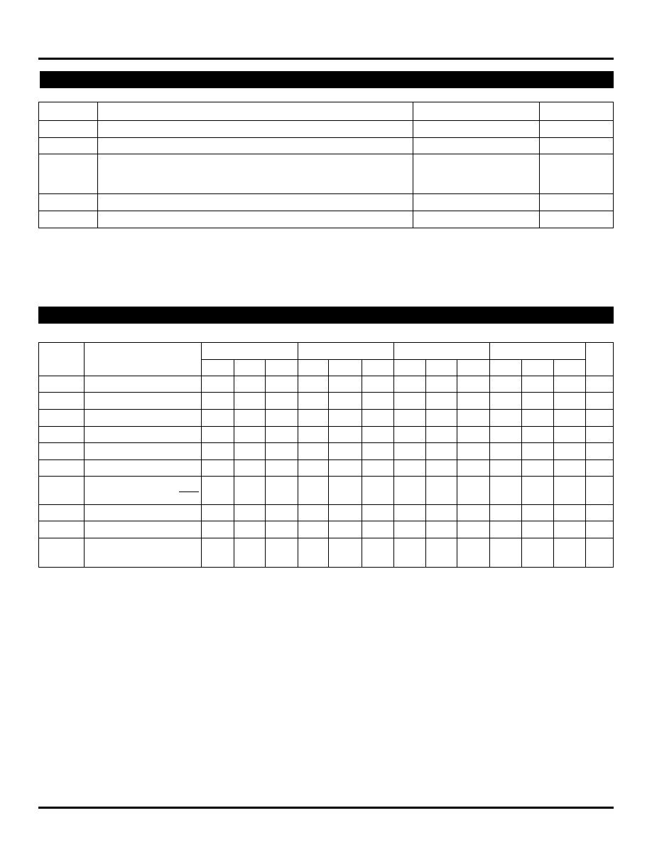
Symbol
Rating
Value
Unit
V
EE
Power Supply (V
CC
= 0V)
-8.0 to 0
VDC
V
I(3)
Input Voltage (V
CC
= 0V)
0 to -6.0
VDC
I
OUT
Output Current
- Continuous
50
mA
- Surge
100
T
A
Operating Temperature Range
-40 to +85
∞
C
V
EE
Operating Range
(1),(2)
-5.7 to -3.0
V
NOTES:
1. Absolute maximum rating, beyond which, device life may be impaired, unless otherwise specified on an individual data sheet.
2. Parametric values specified at:
100EL14V Series:
-3.0V to -5.5V.
3. In PECL mode operation, V
I
(Max) = V
CC
.
ABSOLUTE MAXIMUM RATINGS
(1)
T
A
= ≠40
∞
C
T
A
= 0
∞
C
T
A
= +25
∞
C
T
A
= +85
∞
C
Symbol
Parameter
Min.
Typ.
Max.
Min.
Typ.
Max.
Min.
Typ.
Max.
Min.
Typ.
Max.
Unit
V
OH
Output HIGH Voltage
(2)
-1085 -1005
-880
-1025
-955
-880
-1025
-955
-880
-1025
-955
-880
mV
V
OL
Output LOW Voltage
(2)
-1830 -1695 -1555 -1810 -1705 -1620 -1810 -1705 -1620 -1810 -1705 -1620
mV
V
OHA
Output HIGH Voltage
(2)
-1095
--
--
-1035
--
--
-1035
--
--
-1035
--
--
mV
V
OLA
Output LOW Voltage
(2)
--
--
-1555
--
--
-1610
--
--
-1610
--
--
-1610
mV
V
IH
Input HIGH Voltage
-1165
--
-880
-1165
--
-880
-1165
--
-880
-1165
--
-880
mV
V
IL
Input LOW Voltage
-1810
--
-1475 -1810
--
-1475 -1810
--
-1475 -1810
--
-1475
mV
I
IL
Input LOW Current
(3)
0.5
--
--
0.5
--
--
0.5
--
--
0.5
--
--
µ
A
CLK
-300
--
--
-300
--
--
-300
--
--
-300
--
--
I
IH
Input High Current
--
--
150
--
--
150
--
--
150
--
--
150
µ
A
I
EE
Power Supply Current
--
32
40
--
32
40
--
32
40
--
34
42
mA
V
BB
Output Reference
-1.38
--
-1.26
-1.38
--
-1.26
-1.38
--
-1.26
-1.38
--
-1.26
V
Voltage
DC ELECTRICAL CHARACTERISTICS
V
EE
= V
EE
(Min) to V
EE
(Max); V
CC
= GND
(1)
NOTES:
1. This table replaces the three traditionally seen in ECL 100K data books. The same DC parameter values at V
EE
= -4.5V now apply across the full V
EE
range of -3.0V to -5.5V. Outputs are terminated through a 50
resistor to -2.0V except where otherwise specified on the individual data sheets.
2. V
IN
= V
IH
(Max) or V
IL
(Min).
3. V
IN
= V
IL
(Max).
3
ClockWorksTM
SY100EL14V
Micrel
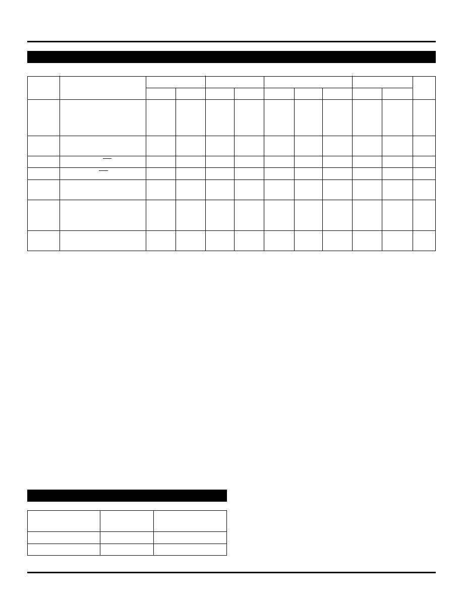
PRODUCT ORDERING CODE
Ordering
Package
Operating
Code
Type
Range
SY100EL14VZC
Z20-1
Commercial
SY100EL14VZCTR
Z20-1
Commercial
T
A
= ≠40
∞
C
T
A
= 0
∞
C
T
A
= +25
∞
C
T
A
= +85
∞
C
Symbol
Parameter
Min.
Max.
Min.
Max.
Min.
Typ.
Max.
Min.
Max.
Unit
t
PLH
Propagation Delay
ps
t
PHL
CLK to Q (Diff)
520
720
550
750
580
680
780
630
830
CLK to Q (SE)
470
770
500
800
530
680
830
580
880
SCLK to Q
470
770
500
800
530
680
830
580
880
t
skew
Part-to-Part Skew
(1)
--
200
--
200
--
--
200
--
200
ps
Within-Device Skew
--
50
--
50
--
--
50
--
50
t
S
Setup Time EN
150
--
150
--
150
--
--
150
--
ps
t
H
Hold Time EN
200
--
200
--
200
--
--
200
--
ps
V
PP
Minimum Input
CLK
150
--
150
--
150
--
--
150
--
mV
Swing
V
CMR
Common Mode Range
(2)
mV
V
PP
< 500mV
-2.0
-0.4
-2.1
-0.4
-2.1
--
-0.4
-2.1
-0.4
V
PP
500mV
-1.8
-0.4
-1.9
-0.4
-1.9
--
-0.4
-1.9
-0.4
t
r
Output Rise/Fall Times
230
500
230
500
230
360
500
230
500
ps
t
f
Q (20% ≠ 80%)
AC ELECTRICAL CHARACTERISTICS
V
EE
= V
EE
(Min) to V
EE
(Max); V
CC
= GND
NOTES:
1. Skews are specified for identical LOW-to-HIGH or HIGH-to-LOW transitions.
2. The V
CMR
range is referenced to the most positive side of the differential input signal. Normal operation is obtained if the HIGH level falls within the specified
range and the peak-to-peak voltage lies between V
PP
(Min) and 1V. The lower end of the V
CMR
range varies 1:1 with V
EE
. The numbers in the specification
table assume a nominal V
EE
= -3.3V. For PECL operation, the V
CMR
(Min) will be fixed at 3.3V ≠ |V
CMR
(Min)|.
4
ClockWorksTM
SY100EL14V
Micrel
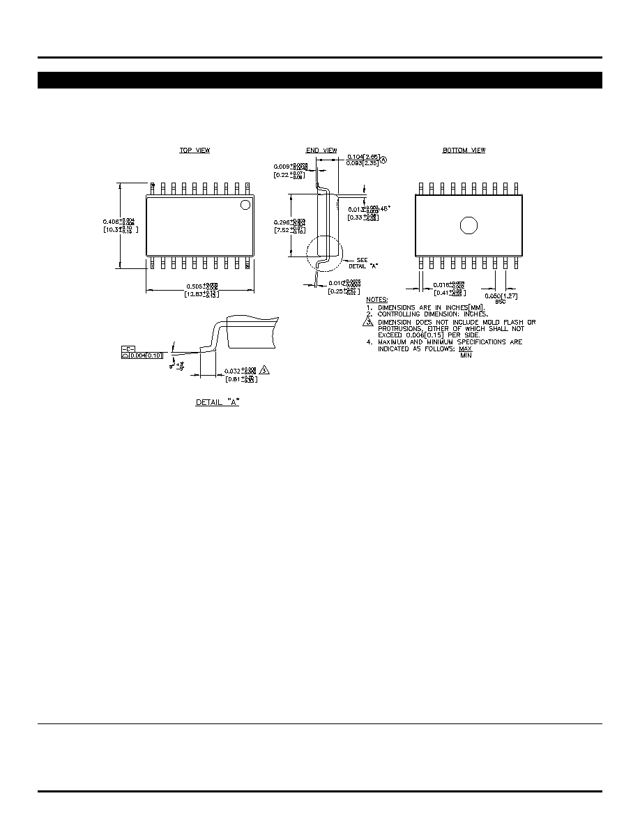
20 LEAD SOIC .300" WIDE (Z20-1)
Rev. 03
MICREL-SYNERGY
3250 SCOTT BOULEVARD
SANTA CLARA
CA 95054
USA
TEL
+ 1 (408) 980-9191
FAX
+ 1 (408) 914-7878
WEB
http://www.micrel.com
This information is believed to be accurate and reliable, however no responsibility is assumed by Micrel for its use nor for any infringement of patents or
other rights of third parties resulting from its use. No license is granted by implication or otherwise under any patent or patent right of Micrel Inc.
© 2000 Micrel Incorporated