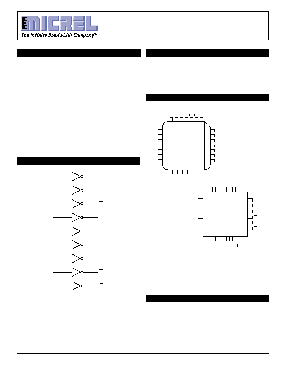
D
9
D
8
V
CCA
V
EE
D
7
D
6
18
17
16
15
14
13
1
2
3
4
5
6
7
24
8
23
9
22
10
21
11
20
12
19
Top View
Flatpack
F24-1
D
1
D
3
D
2
V
CCA
O
3
O
2
V
CC
V
CCA
O
1
O
9
O
8
O
7
D
5
D
4
V
CCA
Q
6
Q
5
Q
4
D
1
O
2
D
2
D
3
O
4
D
4
D
5
O
6
D
6
D
7
O
8
D
8
D
9
O
1
O
3
O
5
O
7
O
9
4
3
2
1
28
27
12
13
14
15
16
17
19
11
20
10
21
9
22
8
23
7
24
6
Top View
PLCC
J28-1
D
6
V
EE
V
CCA
D
7
D
8
V
EES
D
9
26
18
25
5
D
3
V
EES
D
2
V
CCA
D
1
O
3
O
2
V
CCA
V
CC
V
CC
O
9
O
7
O
8
O
1
D
5
D
4
V
CC
A
V
EES
O
4
O
5
O
6
LOW-POWER 9-BIT
INVERTER
s
Max. propagation delay of 700ps
s
I
EE
min. of ≠55mA
s
Extended supply voltage option:
V
EE
= ≠4.2V to ≠5.5V
s
Voltage and temperature compensation for
improved noise immunity
s
70% faster than Fairchild 300K at lower power
s
Internal 75K
input pull-down resistors
s
Function and pinout compatible with Fairchild F100K
s
Available in 24-pin CERPACK and 28-pin PLCC
packages
FEATURES
PIN CONFIGURATIONS
BLOCK DIAGRAM
The SY100S321 is a monolithic 9-bit inverter. The device
contains nine inverting buffer gates with single input and
output.
DESCRIPTION
SY100S321
Rev.: G
Amendment: /0
Issue Date:
July, 1999
Pin
Function
D
1
≠ D
9
Data Inputs
Q
1
≠ Q
9
Data Outputs
V
EES
V
EE
Substrate
V
CCA
V
CCO
for ECL Outputs
PIN NAMES
1
2
SY100S321
Micrel
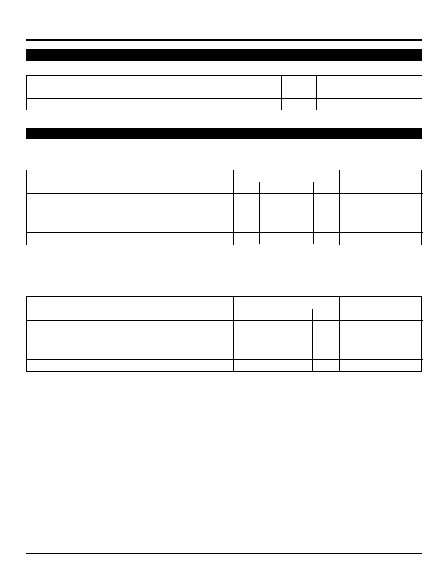
DC ELECTRICAL CHARACTERISTICS
V
EE
= ≠4.2V to ≠5.5V unless otherwise specified, V
CC
= V
CCA
= GND
Symbol
Parameter
Min.
Typ.
Max.
Unit
Condition
I
IH
Input HIGH Current
--
--
200
µ
A
V
IN
= V
IH
(Max.)
I
EE
Power Supply Current
≠55
≠41
≠25
mA
Inputs Open
AC ELECTRICAL CHARACTERISTICS
CERPACK
V
EE
= ≠4.2V to ≠5.5V unless otherwise specified, V
CC
= V
CCA
= GND
T
A
= 0
∞
C
T
A
= +25
∞
C
T
A
= +85
∞
C
Symbol
Parameter
Min.
Max.
Min.
Max.
Min.
Max.
Unit
Condition
t
PLH
Propagation Delay
(1)
300
800
300
800
300
800
ps
t
PHL
Data to Output
t
TLH
Transition Time
(1)
300
900
300
900
300
900
ps
t
THL
20% to 80%, 80% to 20%
t
S
, G≠G
Skew, Gate-to-Gate
--
200
--
200
--
200
ps
NOTE:
1. Reference figures 1 and 2
PLCC
V
EE
= ≠4.2V to ≠5.5V unless otherwise specified, V
CC
= V
CCA
= GND
T
A
= 0
∞
C
T
A
= +25
∞
C
T
A
= +85
∞
C
Symbol
Parameter
Min.
Max.
Min.
Max.
Min.
Max.
Unit
Condition
t
PLH
Propagation Delay
(1)
300
700
300
700
300
700
ps
t
PHL
Data to Output
t
TLH
Transition Time
(1)
300
900
300
900
300
900
ps
t
THL
20% to 80%, 80% to 20%
t
S
, G≠G
Skew, Gate-to-Gate
--
200
--
200
--
200
ps
NOTE:
1. Reference figures 1 and 2
3
SY100S321
Micrel
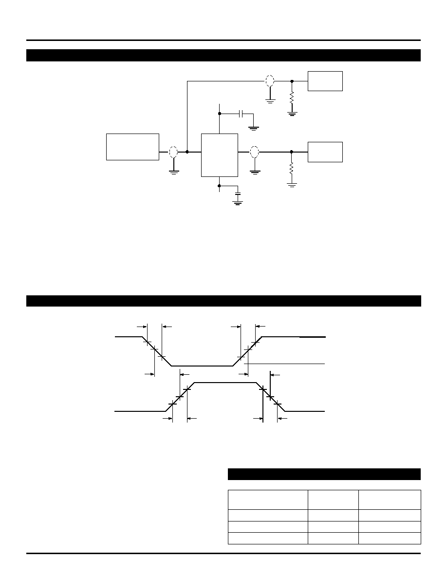
PULSE
GENERATOR
SCOPE
CHAN B
CIRCUIT
UNDER
TEST
SCOPE
CHAN A
R
T
R
T
L1
L2
V
CC
0.1
µ
F
V
EE
0.1
µ
F
Figure 1. AC Test Circuit
TEST CIRCUITRY
(1)
PRODUCT ORDERING CODE
Figure 2. Propagation Delay and Transition Times
SWITCHING WAVEFORMS
NOTE:
1. V
CC
, V
CCA
= +2V, V
EE
= ≠2.5V.
L1 and L2 = equal length 50
impedance lines.
R
T
= 50
terminator internal to scope.
Decoupling 0.1
µ
F from GND to V
CC
and V
EE
.
All unused outputs are loaded with 50
to GND.
C
L
= Fixture and stray capacitance
3pF.
Ordering
Package
Operating
Code
Type
Range
SY100S321FC
F24-1
Commercial
SY100S321JC
J28-1
Commercial
SY100S321JCTR
J28-1
Commercial
INPUT
t
PLH
t
PHL
t
TLH
t
THL
OUTPUT
20%
50%
80%
20%
50%
80%
0.7
±
0.1ns
0.7
±
0.1ns
≠0.95V
≠1.69V
NOTE:
V
EE
= ≠4.2V to ≠5.5V unless otherwise specified, V
CC
= V
CCA
= GND
4
SY100S321
Micrel
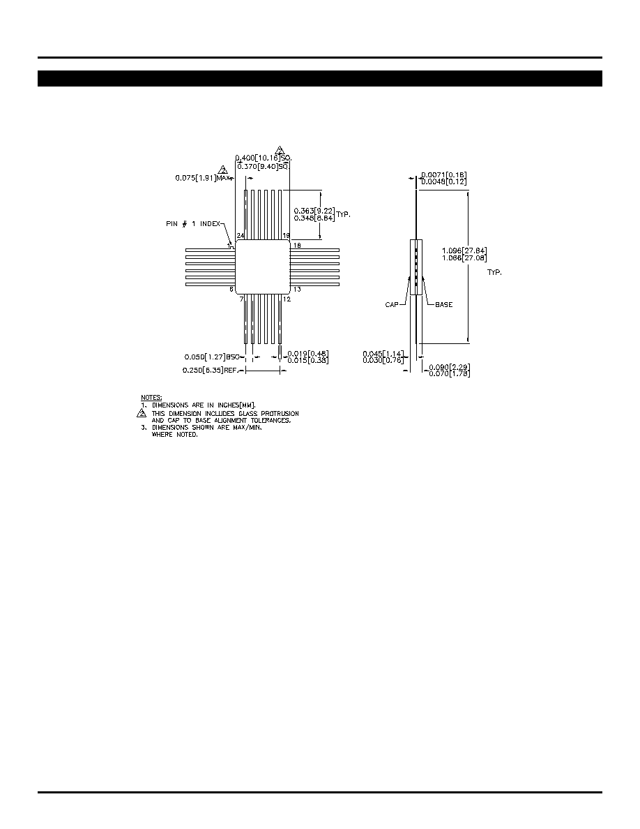
24 LEAD CERPACK (F24-1)
Rev. 03
5
SY100S321
Micrel
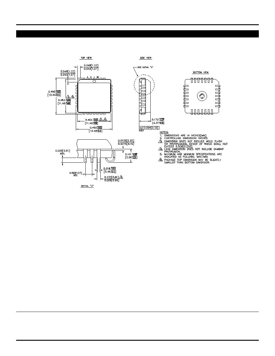
28 LEAD PLCC (J28-1)
Rev. 03
MICREL-SYNERGY
3250 SCOTT BOULEVARD
SANTA CLARA
CA 95054
USA
TEL
+ 1 (408) 980-9191
FAX
+ 1 (408) 914-7878
WEB
http://www.micrel.com
This information is believed to be accurate and reliable, however no responsibility is assumed by Micrel for its use nor for any infringement of patents or
other rights of third parties resulting from its use. No license is granted by implication or otherwise under any patent or patent right of Micrel Inc.
© 2000 Micrel Incorporated