DESCRIPTION
s
High-performance dual 1:10, 1GHz LVDS fanout
buffer/translator
s
Two banks of 10 differential LVDS outputs
s
Guaranteed AC parameters over temperature and
voltage:
∑ > 1GHz f
MAX
∑ < 50ps within device skew
∑ < 400ps t
r
, t
f
time
s
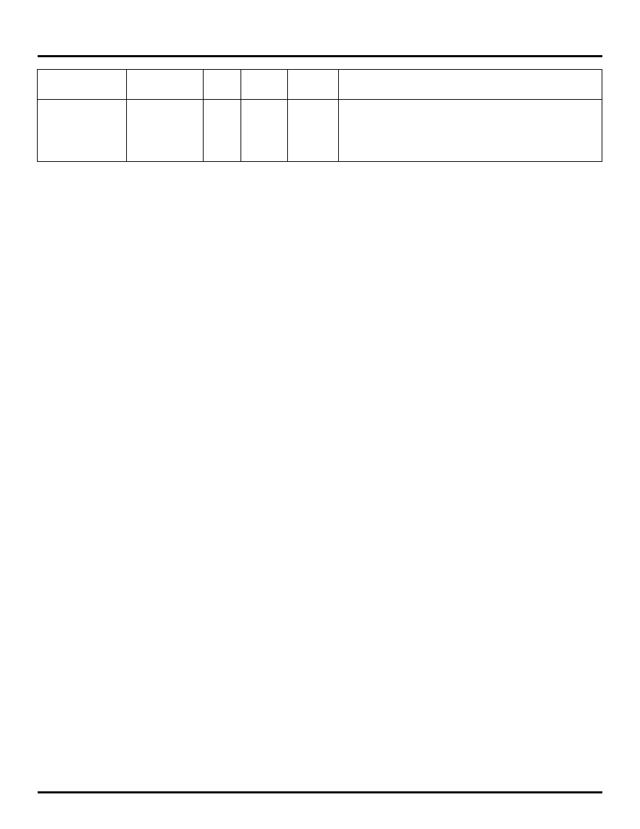
Each bank includes a 2:1 input mux
s
2:1 mux input accepts LVDS and LVPECL
s
Low jitter performance
∑ < 1ps (rms) cycle-to-cycle jitter
∑ < 1ps (pk-pk) total jitter
s
3.3V supply voltage
s
Output enable function
s
LVDS input includes internal 100
termination
s
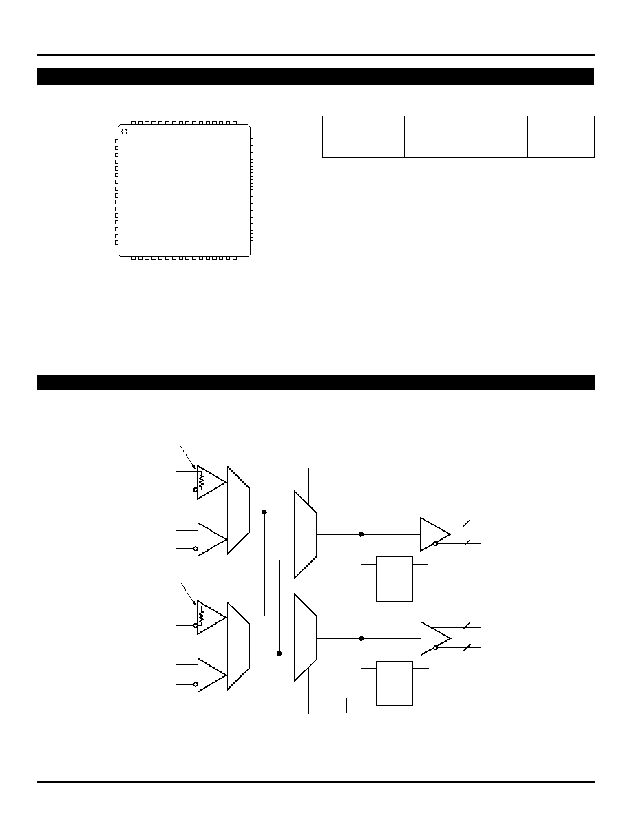
Available in a 64-Pin EPAD-TQFP
FEATURES
3.3V 1GHz DUAL 1:10 PRECISION
LVDS FANOUT BUFFER/
TRANSLATOR WITH 2:1 INPUT MUX
Precision EdgeTM
SY89828L
FINAL
APPLICATIONS
s
Enterprise networking
s
High-end servers
s
Communications
1
Rev.: B
Amendment: /1
Issue Date:
December 2002
The SY89828L is a precision fanout buffer with 20
differential LVDS (Low Voltage Differential Swing) output
pairs. The part is designed for use in low voltage 3.3V
applications that require a large number of outputs to drive
precisely aligned, ultra low-skew signals to their destination.
The input is multiplexed from either LVDS or LVPECL (Low
Voltage Positive Emitter Coupled Logic) by the CLK_SEL1
and CLK_SEL2 pins. The Output Enables (OE1 and OE2)
are synchronous so that the outputs will only be enabled/
disabled when they are already in the LOW state. This
avoids any chance of generating a runt clock pulse when
the device is enabled/disabled as can happen with an
asynchronous control.
The SY89828L features a low pin-to-pin skew of less
than 50ps--performance previously unachievable in a
standard product having such a high number of outputs.
The SY89828L is available in a single space saving package,
enabling a lower overall cost solution.
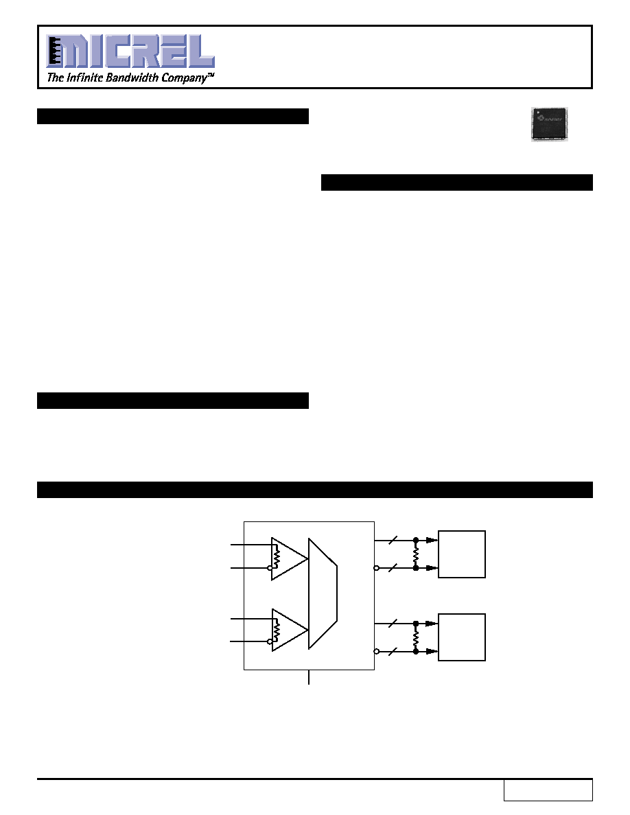
TYPICAL APPLICATION CIRCUIT
SEL1
Primary/Backup Clock Select
(Switchover with 2.0ns)
LVDS_CLKA
/LVDS_CLKA
LVDS_CLKB
/LVDS_CLKB
Primary Clock Source
Backup Clock Source
5
5
5
5
100
100
Primary
Card
Redundant
Card
System using SY89828L as a switchover circuit from a Primary Clock to a Redundant backup Clock in a fail-safe application.
LVPECL inputs not shown in this application.
Precision Edge is a trademark of Micrel, Inc.
Precision EdgeTM
3
Precision EdgeTM
SY89828L
Micrel
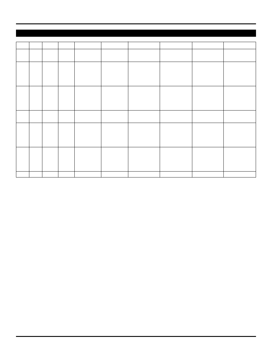
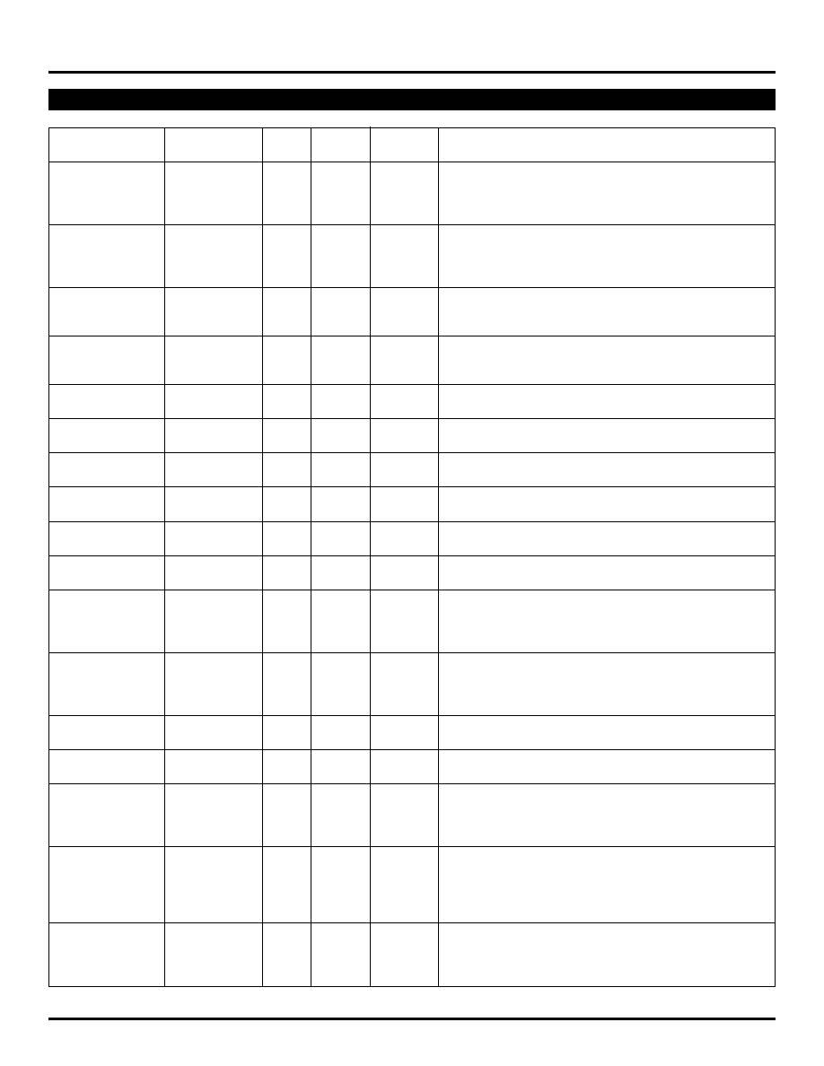
PIN DESCRIPTIONS
Internal
Pin Number
Pin Name
I/O
Type
P/U
Pin Function
5, 6
LVDS_CLKA
Input
LVDS
3.5k
Differential clock input selected by CLK_SEL1, SEL1 and
/LVDS_CLKA
Pull-up
SEL2. Can be left floating if not selected. Floating input, if
See Fig. 2
selected produces an indeterminate output. Has internal
100
termination.
2, 3
LVDS_CLKB
Input
LVDS
3.5k
Differential clock input selected by CLK_SEL1, SEL1 and
/LVDS_CLKB
Pull-up
SEL2. Can be left floating if not selected. Floating input, if
See Fig. 2
selected produces an indeterminate output. Has internal
100
termination.
8, 9
LVPECL_CLKA
Input
LVPECL
75k
Differential clock input selected by CLK_SEL1, SEL1
/LVPECL_CLKA
pull-down
and SEL2. Can be left floating. Floating input, if selected
See Fig. 1
produces a LOW at output. Requires external termination.
12, 13
LVPECL_CLKB
Input
LVPECL
75k
Differential clock input selected by CLK_SEL2, SEL1
/LVPECL_CLKB
pull-down
and SEL2. Requires external termination.
See Fig. 1
7
CLK_SEL1
Input
LVTTL/
11k
Selects LVDS_CLKA input when LOW and
CMOS
Pull-up
LVPECL_CLKA input when HIGH.
14
CLK_SEL2
Input
LVTTL/
11k
Selects LVDS_CLKB input when LOW and
CMOS
Pull-up
LVPECL_CLKB input when HIGH.
16
SEL1
Input
LVTTL/
11k
Selects input source CLKA when LOW and CLKB
CMOS
Pull-up
when HIGH for outputs Q0 ≠ Q9 and /Q0 ≠ /Q9.
1
SEL2
Input
LVTTL/
11k
Selects input source CLKA when LOW and CLKB
CMOS
Pull-up
when HIGH for outputs Q10 ≠ Q19 and /Q10 ≠ /Q19.
11
OE1
Input
LVTTL/
11k
Enable input synchronized internally to prevent output
CMOS
Pull-up
glitches or runt pulses.
15
OE2
Input
LVTTL/
11k
Enable input synchronized internally to prevent output
CMOS
Pull-up
glitches or runt pulses.
4
VCCI
Power
Core VCC connected to 3.3V supply. Not connected to
VCCO internally. Connected to VCCO on PCB.
Bypass with 0.1
µ
F in parallel with 0.01
µ
F low ESR
capacitors as close to VCC pins as possible.
17, 32, 40,
VCCO
Power
Output buffer VCC connected to 3.3V suppy. Not connected
41, 49, 64
to VCCI internally. Connected to VCCI on PCB.
Bypass with 0.1
µ
F in parallel with 0.01
µ
F low ESR
capacitors as close to VCC pins as possible.
10
GNDI
Power
Core ground not connected to GNDO internally.
To be connected to GNDO on PCB.
33, 48
GNDO
Power
Output buffer ground not connected to GNDI internally.
To be connected to GNDI on PCB.
63, 61, 59, 57, 55
Q0 ≠ Q9
Output
LVDS
Differential clock outputs from CLKA when SEL1 = LOW
53, 51, 47, 45, 43
and from CLKB when SEL1 = HIGH. Q outputs are static
when OE1 = LOW. Unused output pair must be terminated
with 100
to maintain low jitter and skew.
62, 60, 58, 56, 54
/Q0 ≠ /Q9
Output
LVDS
Differential clock outputs (complement) from CLKA when
52, 50, 46, 44, 42
SEL1 = LOW and from CLKB when SEL1 = HIGH. /Q
outputs are static HIGH when OE1 = LOW. Unused output
pairs must be externally terminated with 100
to maintain
low jitter and skew.
39, 37, 35, 31, 29
Q10 ≠ Q19
Output
LVDS
Differential outputs from CLKA when SEL2 = LOW and
27, 25, 23, 21, 19
from CLKB when SEL2 = HIGH. Q outputs are static LOW
when OE2 = LOW. Unused output pairs must be externally
terminated with 100
to maintain low jitter and skew.