SY89850U
Precision Low-Power LVPECL Line
Driver/Receiver with Internal Termination
Precision Edge is a trademark of Micrel, Inc.
MicroLeadFrame and MLF are trademarks of Amkor Technology, Inc.
February 2005
M9999-020305
hbwhelp@micrel.com
or (408) 955-1690
General Description
The SY89850U is a 2.5V/3.3V precision, high-speed,
differential receiver capable of handling clocks up to
4GHz and data streams up to 3.2Gbps.
The differential input includes Micrel's unique, 3-pin
input termination architecture that allows users to
interface to any differential signal (AC or DC-coupled)
as small as 100mV (200mV
pp
) without any level
shifting or termination resistor networks in the signal
path. The outputs are 800mV LVPECL, with extremely
fast rise/fall times guaranteed to be less than 160ps.
The SY89850U operates from a 2.5V ±5% supply or a
3.3V ±10% supply and is guaranteed over the full
industrial temperature range of ≠40∞C to +85∞C. The
SY89850U is part of Micrel's high-speed, Precision
EdgeTM product line.
All support documentation can be found on Micrel's
web site at
www.micrel.com
.
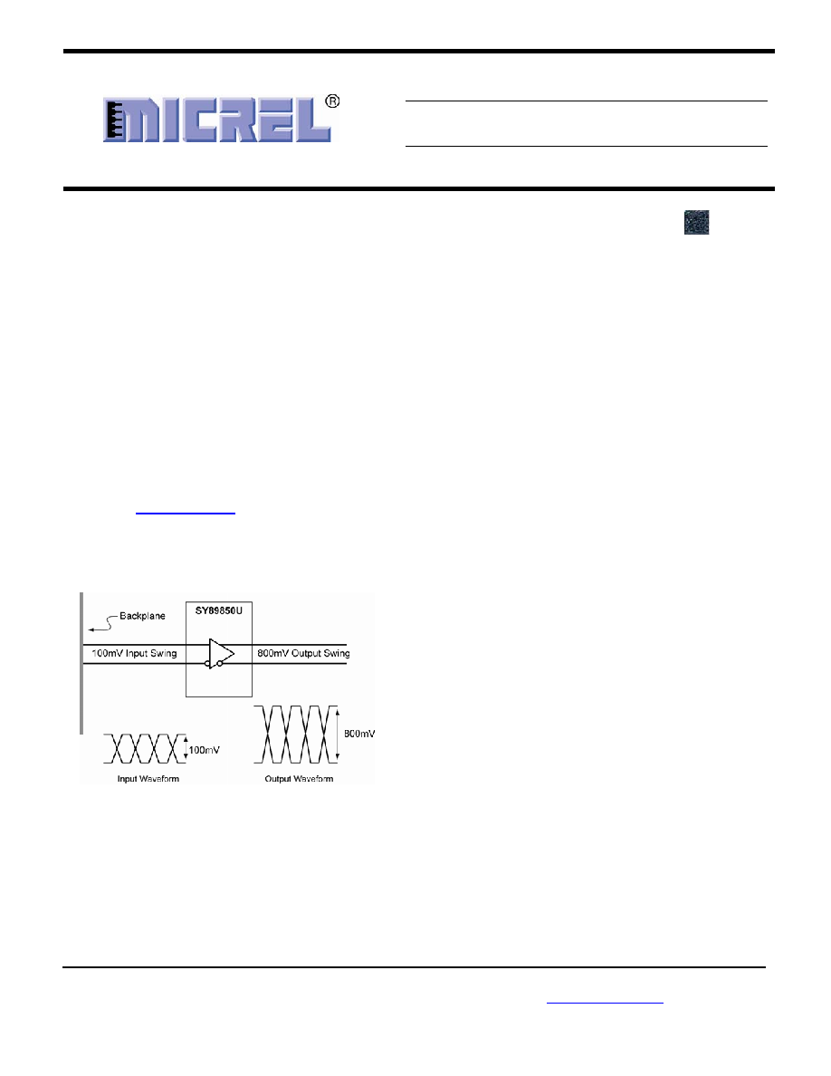
Typical Application
Precision EdgeTM
Features
∑ Guaranteed AC performance over temperature
and supply voltage:
≠ DC- to > 3.2Gbps data rate throughput
≠ 4GHz clock f
max
(typ.)
≠ <280ps In-to-Out t
pd
≠
<160ps
t
r
/t
f
∑ Low power: 50mW (2.5V typ.)
∑ Ultra-low jitter design:
≠ <1ps
(rms)
random jitter
≠ <10ps
(pp)
deterministic jitter
≠ <10ps
(pp)
total jitter (clock)
∑ Unique input termination and VT pin accepts DC-
and AC-coupled inputs (CML, PECL, LVDS)
∑ Typical 800mV (100k) LVPECL Output Swing
∑ Power supply 2.5V ±5% or 3.3V ±10%
∑ Industrial temperature range ≠40∞C to +85∞C
∑ Available in ultra-small (2mm x 2mm) 8-pin
MLFTM package
Applications
∑ Backplane buffering
∑ OC-12 to OC-192 SONET/SDN clock/data
distribution
∑ All Gigabit Ethernet clock or data distribution
∑ Fibre
Channel
distribution
Markets
∑ LAN/WAN
∑ Enterprise Servers
∑ ATE
∑ Test and Measurement

Micrel, Inc.
SY89850U
February 2005
2
M9999-020305
hbwhelp@micrel.com
or (408) 955-1690
Ordering Information
(1)
Part Number
Package
Type
Operating Range
Package Marking
Lead Finish
SY89850UMG
MLF-8
Industrial
850U with Pb-Free bar-line indicator
NiPdAu Pb-Free
SY89850UMGTR
(2)
MLF-8
Industrial
850U with Pb-Free bar-line indicator
NiPdAu Pb-Free
Notes:
1. Contact factory for dice availability. Dice are guaranteed at T
A
= 25∞C, DC Electrical Only.
2. Tape
and
Reel.
Pin Configuration
8-Pin MLFTM (MLF-8)
Pin Description
Pin Number
Pin Name
Pin Function
1, 4
IN, /IN
Differential Input: This input pair is the signal to be buffered. These inputs accept
AC- or DC-coupled signals as small as 100mV. Each pin of this pair internally
terminates to a VT pin through 50. Note that this input will default to an
indeterminate state if left open. Please refer to the "Input Interface Applications"
section for more details.
2 VT
Input Termination Center-Tap: Each side of the differential input pair terminates to
this pin. The VT pin provides a center-tap to a termination network for maximum
interface flexibility. See "Input Interface Applications" section for more details.
3 VREF-AC
Reference Output Voltage: This output biases to V
CC
≠1.2V. Connect to VT pin
when AC-coupling the input. Bypass with 0.01
µF low ESR capacitor to V
CC
.
Maximum sink/source current is ±1.5mA. Due to the limited drive capability, the
VREF-AC pin is only intended to drive its respective VT pin. See "Input Interface
Applications" section.
5
GND,
Exposed Pad
Ground: Ground pin and exposed pad must be connected to the same ground
plane.
7, 6
Q, /Q
Differential 100K LVPECL Output: This LVPECL output is the output of the device.
Terminate through 50 to V
CC
≠2V. See "Output Interface Applications" section.
8
VCC
Positive Power Supply: Bypass with 0.1
µF//0.01µF low ESR capacitors as close to
the VCC pin as possible.
Micrel, Inc.
SY89850U
February 2005
3
M9999-020305
hbwhelp@micrel.com
or (408) 955-1690
Absolute Maximum Ratings
(1)
Supply Voltage (V
CC
) .......................... ≠0.5V to +4.0V
Input Voltage (V
IN
) .................................. ≠0.5V to V
CC
LVPECL Output Current (I
OUT
) ...................................
Continuous..................................................50mA
Surge ........................................................100mA
Input Current ..............................................................
Source or sink current on IN, /IN ..............±50mA
Termination Current ...................................................
Source or sink current on VT ..................±100mA
Source or sink current on V
REF≠AC
.....................±2mA
Lead Temperature (soldering, 20sec.) ............. 260∞C
Storage Temperature (T
s
) ...............≠65∞C to +150∞C
Operating Ratings
(2)
Supply Voltage (V
CC
).................. +2.375V to +2.625V
......................................................+3.0V to +3.6V
Ambient Temperature (T
A
)................ ≠40∞C to +85∞C
Package Thermal Resistance
(3)
MLFTM (
JA
)
Still-Air ..................................................... 93∞C/W
MLFTM (
JB
)
Junction-to-Board .................................... 60∞C/W
DC Electrical Characteristics
(4)
T
A
= ≠40∞C to +85∞C, unless noted.
Symbol Parameter
Condition
Min
Typ
Max Units
V
CC
Power
Supply
2.375
3.0
2.5
3.3
2.625
3.6
V
V
I
CC
Power Supply Current
No load, max. V
CC
20
30
mA
R
DIFF_IN
Differential Input Resistance
(IN-to-/IN)
90
100
110
R
IN
Input Resistance
(IN-to-V
T
), (/IN-to-V
T
)
45
50
55
V
IH
Input High Voltage
(IN, /IN)
Note 5
V
CC
≠1.6 V
CC
V
V
IL
Input Low Voltage
(IN, /IN)
0
V
IH
≠0.1 V
V
IN
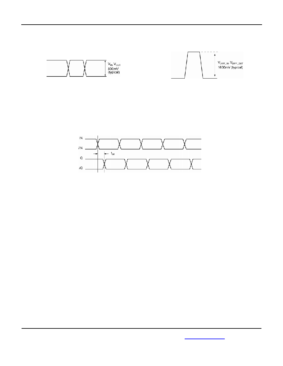
Input Voltage Swing
(IN, /IN)
See Figure 1a.
0.1
1.7
V
V
DIFF_IN
Differential Input Voltage Swing
|IN≠/IN|
See Figure 1b.
0.2
V
V
T_IN
In-to-V
T
(IN, /IN)
1.28
V
V
REF≠AC
Output Reference Voltage
V
CC
≠1.3 V
CC
≠1.2 V
CC
≠1.1 V
Notes:
1.
Permanent device damage may occur if Absolute Maximum Ratings are exceeded. This is a stress rating only and functional operation is
not implied at conditions other than those detailed in the operational sections of this data sheet. Exposure to absolute maximum rating
conditions for extended periods may affect device reliability.
2.
The data sheet limits are not guaranteed if the device is operated beyond the operating ratings.
3.
Package Thermal Resistance assumes exposed pad is soldered (or equivalent) to the devices most negative potential on the PCB.
4.
The circuit is designed to meet the DC specifications shown in the above table after thermal equilibrium has been established.
5. V
IH
(min) not lower than 1.2V.
Micrel, Inc.
SY89850U
February 2005
4
M9999-020305
hbwhelp@micrel.com
or (408) 955-1690
LVPECL Output DC Electrical Characteristics
(6)
V
CC
= +2.5V ±5% or +3.3V ±10%; T
A
= ≠40∞C to +85∞C; R
L
= 50 to V
CC
≠2V, unless otherwise stated.
Symbol Parameter
Condition
Min
Typ
Max Units
V
CC
Output High Voltage
Q, /Q
V
CC
≠1.145
V
CC
≠0.895
V
V
OL
Output Low Voltage
Q, /Q
V
CC
≠1.945
V
CC
≠1.695
V
V
OUT
Output Voltage Swing
Q, /Q
See Figure 1a.
550
800
mV
V
DIFF_OUT
Differential Output Voltage Swing
Q, /Q
See Figure 1b.
1100
1600
mV
Note:
6.
The circuit is designed to meet the DC specifications shown in the above table after thermal equilibrium has been established.
AC Electrical Characteristics
(7)
V
CC
= +2.5V ±5% or +3.3V ±10%; T
A
= ≠40∞C to +85∞C; R
L
= 50 to V
CC
≠2V, unless otherwise stated.
Symbol Parameter
Condition
Min
Typ Max Units
NRZ Data
3.2
Gbps
f
MAX
Maximum Operating Frequency
V
OUT
400mV Clock
4
GHz
t
pd
Propagation Delay
IN-to-Q
V
IN
100mV
180
260
360
ps
t
pd
Tempco
Differential Propagation Delay
Temperature Coefficient
115
fs/∞C
Note 8
1
ps
(rms)
t
JITTER
Data
Random Jitter (RJ)
Deterministic Jitter (DJ)
Note 9
10
ps
(pp)
Note 10
1
ps
(rms)
Clock
Cycle-to-Cycle Jitter
Total Jitter (TJ)
Note 11
10
ps
(pp)
t
r
, t
f
Rise/Fall Time (20% to 80%)
Q, /Q
At full output swing.
50
100
160
ps
Notes:
7.
The circuit is designed to meet the AC specifications shown in the above table after thermal equilibrium has been established.
8.
Random jitter is measured with a K28.7 comma detect character pattern, measured at 2.5Gbps and 3.2Gbps.
9. Deterministic jitter is measured at 2.5Gbps and 3.2Gbps, with both K28.5 and 2
23
≠1 PRBS pattern.
10. Cycle-to-cycle jitter definition: the variation of periods between adjacent cycles, T
n
≠T
n-1
where T is the time between rising edges of the
output signal.
11. Total jitter definition: with an ideal clock input of frequency < f
MAX
, no more than one output edge in 10
12
output edges will deviate by more
than the specified peak-to-peak jitter value.
Micrel, Inc.
SY89850U
February 2005
5
M9999-020305
hbwhelp@micrel.com
or (408) 955-1690
Single-Ended and Differential Swings
Figure 1a. Singled-Ended Voltage Swing
Figure 1b. Differential Voltage Swing
Timing Diagram