PDSP16318/16318A
1
Supersedes version DS3708 - 2.4 September 1996
DS3708 - 3.1 November 1998
PDSP16318/PDSP16318A
Complex Accumulator
Advance Information
The PDSP16318/A contains two independent 20-bit
Adder/Subtractors combined with accumulator registers and
shift structures. The four port architecture permits full 20MHz
throughout in FFT and filter applications.
Two PDSP16318As combined with a single PDSP16112A
Complex Multiplier provide a complete arithmetic solution for
a Radix 2 DIT FFT Butterfly. A new complex Butterfly result
can be generated every 50ns allowing 1K complex FFTs to be
executed in 256
µ
s.
FEATURES
s
Full 20MHz Throughout in FFT Applications
s
Four Independent 16-bit I/O Ports
s
20-bit Addition or Accumulation
s
Fully Compatible with PDSP16112 Complex Multiplier
s
On Chip Shift Structures for Result Scaling
s
Overflow Detection
s
Independent Three-State Outputs and Clock
Enables for 2 Port 20MHz Operation
s
1.4 micron CMOS
s
500mW Maximum Power Dissipation
s
100 CQFP package
APPLICATIONS
s
High speed Complex FFT or DFTs
s
Complex Finite Impulse Response (FIR) Filtering
s
Complex Conjugation
s
Complex Correlation/Convolution
ASSOCIATED PRODUCTS
PDSP16112 16 x 12 Complex Multiplier
PDSP16116 16 x 16 Complex Multiplier
PDSP1601
ALU and Barrel Shifter
PDSP16330 Pythagoras Processor
Fig.1 Pin connections - Top view (GC100)
GC100
ORDERING INFORMATION
Industrial (-40
∞
C to +85
∞
C)
PDSP16318A/IG/GC1R
(20MHz - QFP)
Military (-55
∞
C to +125
∞
C)
PDSP16318/MC/GC1R
(10MHz - QFP
MIL STD 883C Screened)
N.B. Further details of the Military grade part are available
in a separate datasheet
Fig. 2 PDSP16318 simplified block diagram
REG
DELAY
A
B
B
A
SHIFT
REG
C
A
B
SHIFT
REG
D
REG
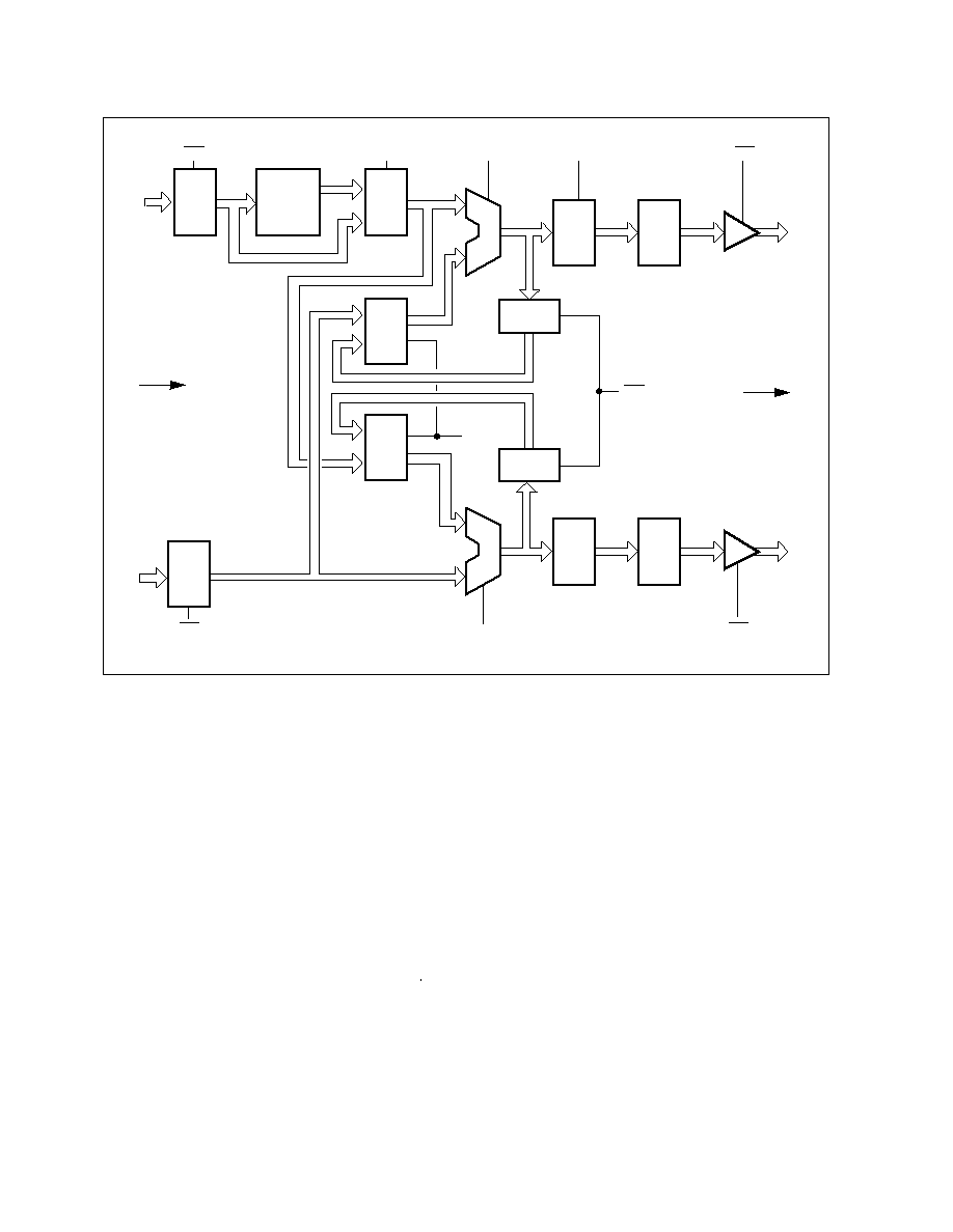
PDSP16318/16318A
2
A
B
SHIFT
REG
REG
D
B
A
SHIFT
REG
D
MUX
MUX
MUX
A REG
CYCLE
DELAY
REG
REG
A
16
16
8
20
20
20
16
16
16
16
20
16
16
B
20
20
20
MS
CEB
ASI
OED
CLR
OVR
OEC
S2:0
ASR
DEL
CEA
CLK
Fig. 3 Block diagram
PDSP16318/16318A
3
FUNCTIONAL DESCRIPTION
The PDSP16318 is a Dual 20-bit Adder/Subtractor
configured to support Complex Arithmetic. The device may be
used with each of the adders allocated to real or imaginary
data (e.g. Complex Conjugation), the entire device allocated
to Real or Imaginary Data (e.g. Radix 2 Butterflys) or each of
the adders configured as accumulators and allocated to real
or imaginary data (Complex Filters). Each of these modes
ensures that a full 20MHz throughput is maintained through
both adders, the first and last mode illustrating true Complex
operation, where both real and imaginary data is handled by
the single device.
Both Adder/Subtractors may be controlled
independently via the ASR and ASI inputs. These controls
permit A + B, A - B, B - A or pass A operations, where the A
input to the Adder is derived from the input multiplexer. The
CLR
control line allows the clearing of both accumulator
registers. The two multiplexers may be controlled via the MS
inputs, to select either new input data, or fed-back data from
the accumulator registers. The PDSP16318 contains an 8-
cycle deskew register selected via the DEL control. This
deskew register is used in FFT applications to ensure correct
phasing of data that has not passed through the PDSP16112
Complex Multiplier.
The 16-bit outputs from the PDSP16318 are derived from
the 20-bit result generated by the Adders. The three bit S2:0
input selects eight different shifted output formats ranging
from the most significant 16 bits of the 20-bit data, to the least
significant 13 bits of the 20-bit data. In this mode the 14th, 15th
and 16th bits of the output are set to zero. The shift selected
is applied to both adder outputs, and determines the function
of the OVR flag. The OVR flag becomes active when either of
the two adders produces a result that has more significant
digits than the MSB of the 16-bit output from the device. In this
manner all cases when invalid data appears on the output are
flagged.
Symbol
A15:0
B15:0
C15:0
D15:0
CLK
CEA
CEB
OEC
OED
OVR
ASR1:0
ASI1:0
CLR
MS
S2:0
DEL
VCC
GND
Description
Data presented to this input is loaded into the input register on the rising edge of CLK. A15 is the MSB.
Data presented to this input is loaded into the input register on the rising edge of CLK. B15 is the MSB
and has the same weighting as A15.
New data appears on this output after the rising edge of CLK. C15 is the MSB.
New data appears on this output after the rising edge of CLK. C15 is the MSB.
Common Clock to all internal registers
Clock enable: when low the clock to the A input register is enabled.
Clock enable: when low the clock to the B input register is enabled.
Output enable: Asynchronous 3-state output control: The C outputs are in a high impedance
state when this input is high.
Output enable: Asynchronous 3-state output control: The D outputs are in a high impedance
state when this input is high.
Overflow flag: This flag will go high in any cycle during which either the output data overflows the number
range selected or either of the adder results overflow. A new OVR appears after the rising edge of the
CLK.
Add/subtract Real: Control input for the 'Real' adder. This input is latched by the rising edge of clock.
Add/subtract Imag: Control input for the 'Imag' adder. This input is latched by the rising edge of clock.
Accumulator Clear: Common accumulator clear for both Adder/Subtractor units. This input is latched by
the rising edge of CLK.
Mux select: Control input for both adder multiplexers. This input is latched by the rising edge of CLK.
When high the feedback path is selected.
Scaling control: This input selects the 16-bit field from the 20-bit adder result that is routed to the outputs.
This input is latched by the rising edge of CLK.
Delay Control: This input selects the delayed input to the real adder for operations involving the
PDSP16112. This input is latched by the rising edge of CLK.
+5V supply: Both Vcc pins must be connected.
0V supply: Both GND pins must be connected.
Type
Input
Input
Output
Output
Input
Input
Input
Input
Input
Output
Input
Input
Input
Input
Input
Input
Power
Ground
PDSP16318/16318A
4
GC pin
77
82
83
84
85
86
87
88
89
90
91
92
93
94
95
96
97
98
99
100
5
Function
D7
D8
D9
D10
GND
VCC
D11
D12
D13
D14
D15
C15
C14
C13
C12
VCC
GND
C11
C10
C9
C8
GC pin
6
7
8
9
10
11
12
13
14
15
16
17
18
19
20
21
22
23
24
25
26
Function
C7
C6
C5
C4
C3
C2
C1
C0
OED
OEC
S2
S1
S0
MS
ASI1
ASI0
DEL
CLR
ASR1
ASR0
A0
GC pin
31
32
33
34
35
36
37
38
39
40
41
42
43
44
45
46
47
48
49
50
51
Function
A1
A2
A3
A4
A5
A6
A7
A8
A9
A10
A11
A12
A13
A14
A15
CEA
B15
B14
B13
B12
B11
GC pin
56
57
58
59
60
61
62
63
64
65
66
67
68
69
70
71
72
73
74
75
76
Function
B10
B9
B8
B7
B6
B5
B4
B3
B2
B1
B0
CLK
CEB
OVR
D0
D1
D2
D3
D4
D5
D6
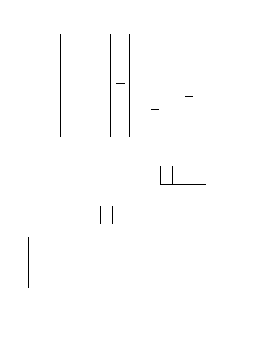
Device Pinout for ceramic QFP (GC100)
ASX1
0
0
1
1
ASR or ASI
ASX0
0
1
0
1
A + B
A
A - B
B - A
ALU Function
MS
0
1
Real and Imag' Mux Control
B port input/Del mux output
C accumulator/D accumualtor
DEL
0
1
Delay Mux Control
A port input
Delayed A port input
S2
0
0
0
0
1
1
1
1
S1
0
0
1
1
0
0
1
1
S0
0
1
0
1
0
1
0
1
19
15
18
14
15
17
13
14
15
16
12
13
14
15
15
11
12
13
14
15
14
10
11
12
13
14
15
13
9
10
11
12
13
14
15
12
8
9
10
11
12
13
14
15
11
7
8
9
10
11
12
13
14
10
6
7
8
9
10
11
12
13
9
5
6
7
8
9
10
11
12
8
4
5
6
7
8
9
10
11
7
3
4
5
6
7
8
9
10
6
2
3
4
5
6
7
8
9
5
1
2
3
4
5
6
7
8
4
0
1
2
3
4
5
6
7
3
0
1
2
3
4
5
6
2
0
1
2
3
4
5
1
0
1
2
3
4
0
0
1
2
3
S2:0
Adder result
NOTE
This table shows the portion of the adder result passed to the D15:0 and C15:0 outputs. Where fewer than 16 adder bits are selected
the output data is padded with zeros.
PDSP16318/16318A
5
ABSOLUTE MAXIMUM RATINGS
(Note 1)
Supply voltage V
CC
-0.5V to 7.0V
Input voltage V
IN
-0.9V to V
CC
+0.9V
Output voltage V
OUT
-0.9V to V
CC
+0.9V
Clamp diode current per pin I
k
(see Note 2)
18mA
Static discharge voltage (HMB) V
STAT
500V
Storage temperature range T
S
-65
∞
C to +150
∞
C
Ambient temperature with
power applied T
amb
Industrial
-40
∞
C to +85
∞
C
Military
-55
∞
C to +125
∞
C
Junction temperature
150
∞
C
Package power dissipation P
TOT
1000mW
NOTES
1.
Exceeding these ratings may cause permanent damage.
Functional operation under these conditions is not implied.
2.
Maximum dissipation or 1 second should not be exceeded, only
one output to be tested at any one time.
3.
Exposure to absolute maximum ratings for extended periods may
affect device reliability.
THERMAL CHARACTERISTICS
Package Type
GC
JC
∞
C/W
12
JA
∞
C/W
35
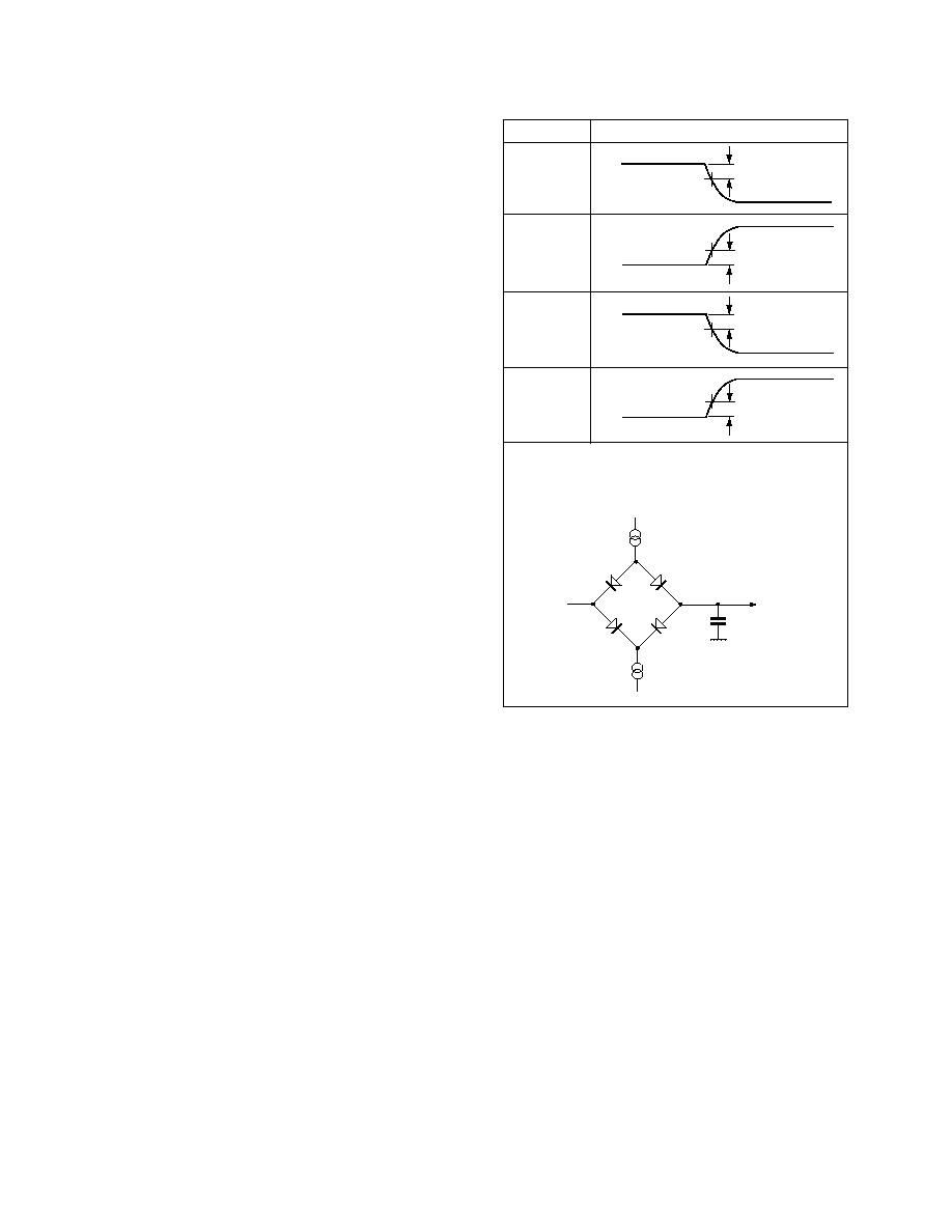
0.5V
0.5V
0.5V
0.5V
VH
VL
1.5V
1.5V
Delay from output
low to output
high impedance
Delay from output
high impedance to
Output low
Delay from output
high to output
high impedance
Delay from output
high impedance to
Output high
NOTES
1. VH - Voltage reached when output driven high
2. VL - Voltage reached when output driven low
Test
Waveform - measurement level
DUT
100p
I
OH
1.5V
I
OL
PDSP16318/16318A
6
Min.
100
20
20
8
2
10
8
2
2
8
5
-
-
-
-
-
Max.
-
-
-
-
-
-
-
-
-
-
30
30
30
30
110
60
Min.
50
15
15
5
2
10
5
2
2
8
5
-
-
-
-
-
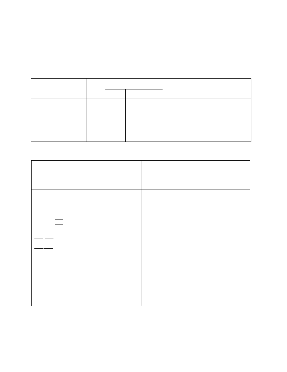
ELECTRICAL CHARACTERISTICS
Test conditions (unless otherwise stated):
T
amb
(Commercial) = 0
∞
C to +70
∞
C, V
CC
= 5.0V
±
5%, GND = 0V
T
amb
(Industrial) =-40
∞
C to +85
∞
C, V
CC
= 5.0V
±
10%, GND = 0V
T
amb
(Military) =-55
∞
C to +125
∞
C, V
CC
= 5.0V
±
10%, GND = 0V
STATIC CHARACTERISTICS
Value
Characteristic
Symbol
Units
Conditions
Min.
Typ.
Max.
Output high voltage
V
OH
2.4
-
V
I
OH
= 3.2mA
Output low voltage
V
OL
-
0.4
V
l
OL
=-3.2mA
Input high voltage
V
IH
3.5
-
V
Input low voltage
V
IL
-
0.5
V
Input leakage current
I
IL
-10
+10
µ
A
GND < V
IN
<V
CC
Output leakage current
l
oz
-50
-
+50
µ
A
GND <V
OUT
< V
CC
Output SC current
I
OS
20
-
200
mA
V
cc
= Max
Input capacitance
C
IN
-
9
-
pF
Max.
-
-
-
-
-
-
-
-
-
-
40
40
40
40
70
30
Characteristic
Clock period
Clock High Time
Clock Low Time
A15:0, B15:0 setup to clock rising edge
A15:0, B15:0 hold after clock rising edge
MS, S2:0, ASI setup to clock rising edge
DEL, ASR,
CLR
setup to clock rising edge
DEL, ASR,
CLR
, MS, S2:0, ASI hold after
clock rising edge
CEA
,
CEB
setup to clock falling edge
CEA
,
CEB
hold after clock rising edge
Clock rising edge to OVR, C15:0, D15:0
OEC
/
OED
low to C15:0/D15:0 high data valid
OEC
/
OED
low to C15:0/D15:0 low data valid
OEC
/
OED
high to C15:0/D15:0 high impedance
Vcc current
Vcc current
Conditions
2 x LSTTL + 20pF
2 x LSTTL + 20pF
2 x LSTTL + 20pF
2 x LSTTL + 20pF
V
CC
= max,
TTL input levels
Outputs unloaded,
f
CLK
= max
V
CC
= max,
CMOS input levels
Outputs unloaded,
f
CLK
= max
SWITCHING CHARACTERISTICS
Units
ns
ns
ns
ns
ns
ns
ns
ns
ns
ns
ns
ns
ns
ns
mA
mA
PDSP16318
PDSP16318A
Value
Industrial
Value
Military
NOTES
1.
LSTTL is equivalent to I
OH
= 20 microamps, I
OL
= -0.4mA
2.
Current is defined as negative into the device
3.
CMOS input levels are defined as:
V
IL
= 0.5
V
IH
= V
DD
- 0.5

M Mitel (design) and ST-BUS are registered trademarks of MITEL Corporation
Mitel Semiconductor is an ISO 9001 Registered Company
Copyright 1999 MITEL Corporation
All Rights Reserved
Printed in CANADA
TECHNICAL DOCUMENTATION - NOT FOR RESALE
World Headquarters - Canada
Tel: +1 (613) 592 2122
Fax: +1 (613) 592 6909
North America
Asia/Pacific
Europe, Middle East,
Tel: +1 (770) 486 0194
Tel: +65 333 6193
and Africa (EMEA)
Fax: +1 (770) 631 8213
Fax: +65 333 6192
Tel: +44 (0) 1793 518528
Fax: +44 (0) 1793 518581
http://www.mitelsemi.com
Information relating to products and services furnished herein by Mitel Corporation or its subsidiaries (collectively "Mitel") is believed to be reliable. However, Mitel assumes no
liability for errors that may appear in this publication, or for liability otherwise arising from the application or use of any such information, product or service or for any infringement of
patents or other intellectual property rights owned by third parties which may result from such application or use. Neither the supply of such information or purchase of product or
service conveys any license, either express or implied, under patents or other intellectual property rights owned by Mitel or licensed from third parties by Mitel, whatsoever.
Purchasers of products are also hereby notified that the use of product in certain ways or in combination with Mitel, or non-Mitel furnished goods or services may infringe patents or
other intellectual property rights owned by Mitel.
This publication is issued to provide information only and (unless agreed by Mitel in writing) may not be used, applied or reproduced for any purpose nor form part of any order or
contract nor to be regarded as a representation relating to the products or services concerned. The products, their specifications, services and other information appearing in this
publication are subject to change by Mitel without notice. No warranty or guarantee express or implied is made regarding the capability, performance or suitability of any product or
service. Information concerning possible methods of use is provided as a guide only and does not constitute any guarantee that such methods of use will be satisfactory in a specific
piece of equipment. It is the user's responsibility to fully determine the performance and suitability of any equipment using such information and to ensure that any publication or
data used is up to date and has not been superseded. Manufacturing does not necessarily include testing of all functions or parameters. These products are not suitable for use in
any medical products whose failure to perform may result in significant injury or death to the user. All products and materials are sold and services provided subject to Mitel's
conditions of sale which are available on request.