F o r W i n d o w s
Æ
C E A p p l i c a t i o n s
Designed around the popular MIPS
architecture, the V
R
4300 offers one
of the best MIPS performance/die
size solutions on the market. Its
internal operating frequency is either
100 MHz or 133 MHz at 3.3V. The
V
R
4300 CPU has an optimized five-
stage pipeline, 16K instruction cache,
8K data cache, memory management
unit, floating-point arithmetic unit
(FPU) and clock generator. The
V
R
4300 is one of the most powerful
processors available to support
Windows CE, making it ideal for many
performance-intensive tethered
applications.
V
R
4 3 0 0
TM
6 4 - B I T M I P S
Æ
R I S C M I C R O P R O C E S S O R
S A L I E N T F E A T U R E S
F E A T U R E D E S C R I P T I O N
--
64-bit MIPS RISC architecture
--
133 or 100 MHz operation
--
Conformance to MIPS I/II/III instruction
set architectures
--
Five-stage pipeline processing
--
High-speed execution of integer and
floating-point operations
--
Performance levels of 80/60 SPECint92
(133MHz) and 60/45 SPECfp92 (100MHz)
--
Same input clock as system bus frequency
--
16K instruction cache and 8K data
cache
--
Multiplexed 32-bit address/data bus
--
Low power dissipation: 1.8 W typical
and 2.2 W maximum
--
Supply voltage of 3.3 volts
--
120-pin plastic QFP packaging
Execution Unit
--
64-bit register file
--
64-bit integer/mantissa data bus
--
12-bit exponent data bus
Co-Processor
--
Exception processing unit with system control co-processor registers
--
Memory management unit that converts virtual addresses into physical addresses and
verifies memory access of kernel, supervisor and user memory segments
--
Seven page sizes: 4K, 16K, 64K, 256K, 1M, 4M and 16M (VSIZE=40 and PSIZE=32)
--
Translation lookaside buffer with 32 entries, each mapped to an even or odd frame buffer page
Cache Memory Unit
--
16K direct-mapped instruction cache and 8K data cache
--
Write-back cache for reducing store operations
Pipeline Control
--
Occurrence of cache misses
--
Flash buffer full
--
Multicycle instructions
--
Occurrence of system exceptions
Floating-Point Arithmetic Unit
--
Integrated into CPU's integer arithmetic unit
--
32-bit (single-precision) and 64-bit (double-precision)
IEEE 754 floating-point arithmetic support
Clock Generator
--
Four clocks generated from MasterClock input
--
Phase-locked loop (PLL) to suppress skew between the input clock and internal clock
High Performance
--
60 SPECint92, 45 SPECfp92, 131 MIPS (100MHz)
--
80 SPECint92, 60 SPECfp92, 173 MIPS (133MHz)
Low Power Consumption
--
1.8W typical @ 100MHz, 3.3V
--
2.4W typical @ 133MHz, 3.3V
Control
Master
Clock
Data
Address
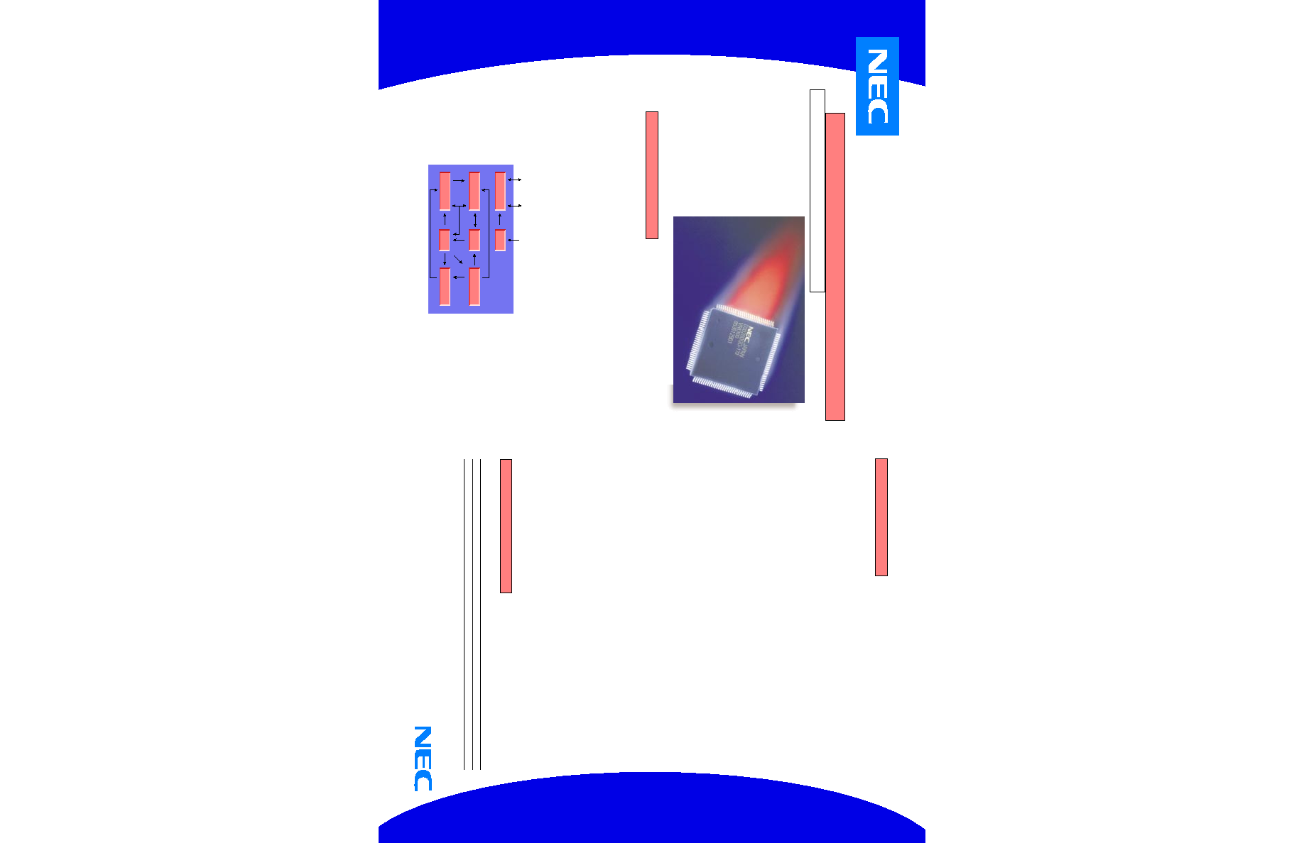
System Interface
Instruction Cache
Instruction Address
Pipeline Control
CPO
TLB
Clock
Generator
Data
Cache
Execution
Unit
© 1997 NEC Electronics Inc.
Subject to change without notice. All rights reserved. V
R
4100, V
R
4102, V
R
4300 and V
R
Series are trademarks of NEC Corporation.
MIPS is a registered trademark of MIPS Group, a division of Silicon Graphics, Inc. Microsoft, Windows and Windows CE are either
trademarks or registered trademarks of Microsoft Corporation in the United States and/or other countries. CompactFlash is a
trademark of the CompactFlash Association. Miniature Card is a trademark of the Miniature Card Implementers Forum. All other
registered marks or trademarks are property of their respective holder. Printed in the USA.. 50843
O R D E R I N G I N F O R M A T I O N
PART NUMBER
PACKAGE
µPD30200GD-100-MBB
120-pin QFP (28mmx28mm) 100 MHz
µPD30200GD-133-MBB
120-pin QFP (28mmx28mm) 133 MHz