 | –≠–ª–µ–∫—Ç—Ä–æ–Ω–Ω—ã–π –∫–æ–º–ø–æ–Ω–µ–Ω—Ç: 54F132FM | –°–∫–∞—á–∞—Ç—å:  PDF PDF  ZIP ZIP |

54F/74F132
Quad 2-Input NAND Schmitt Trigger
General Description
The 'F132 contains four 2-input NAND gates which accept
standard TTL input signals and provide standard TTL output
levels. They are capable of transforming slowly changing in-
put signals into sharply defined, jitter-free output signals. In
addition, they have a greater noise margin than conventional
NAND gates.
Each circuit contains a 2-input Schmitt trigger followed by
level shifting circuitry and a standard FAST
Æ
output struc-
ture. The Schmitt trigger uses positive feedback to effectively
speed-up slow input transitions, and provide different input
threshold voltages for positive and negative-going transi-
tions. This hysteresis between the positive-going and
negative-going input threshold (typically 800 mV) is deter-
mined by resistor ratios and is essentially insensitive to tem-
perature and supply voltage variations.
Features
n
Guaranteed 4000V minimum ESD protection
n
Standard Military Drawing (SMD)
n
5962-89487
Ordering Code:
See Section 0
Commercial
Military
Package
Package Description
Number
74F132PC
N14A
14-Lead (0.300" Wide) Molded Dual-In-Line
54F132DM (Note 2)
J14A
14-Lead Ceramic Dual-In-Line
74F132SC (Note 1)
M14A
14-Lead (0.150" Wide) Molded Small Outline, JEDEC
74F132SJ (Note 1)
M14D
14-Lead (0.300" Wide) Molded Small Outline, EIAJ
54F132FM (Note 2)
W14B
14-Lead Cerpack
54F132LM (Note 2)
E20A
20-Lead Ceramic Leadless Chip Carrier, Type C
Note 1: Devices also available in 13" reel. Use suffix = SCX and SJX.
Note 2: Military grade device with environmental and burn-in processing. Use suffix = DMQB, FMQB and LMQB.
Logic Symbol
TRI-STATE
Æ
is a registered trademark of National Semiconductor Corporation.
IEEE/IEC
DS009477-3
November 1994
54F/74F132
Quad
2-Input
NAND
Schmitt
T
rigger
54F/74F132
© 1997 National Semiconductor Corporation
DS009477
www.national.com
1
PrintDate=1997/08/28 PrintTime=12:25:28 10193 ds009477 Rev. No. 1
cmserv
Proof
1
DSXXX
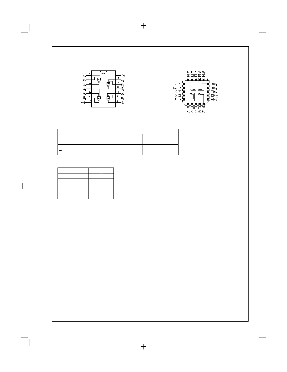
Connection Diagrams
Unit Loading/Fan Out
See Section 0 for U.L. definitions
54F/74F
Pin Names
Description
U.L.
Input I
IH
/I
IL
HIGH/LOW
Output I
OH
/I
OL
A
n
, B
n
Inputs
1.0/1.0
20 µA/-0.6 mA
O
n
Outputs
50/33.3
-1 mA/20 mA
Function Table
Inputs
Outputs
A
B
O
L
L
H
L
H
H
H
L
H
H
H
L
H = HIGH Voltage Level
L = LOW Voltage Level
Pin Assignment for
DIP, SOIC and Flatpak
DS009477-1
Pin Assignment
for LCC
DS009477-2
PrintDate=1997/08/28 PrintTime=12:25:31 10193 ds009477 Rev. No. 1
cmserv
Proof
2
DSXXX
www.national.com
2

Absolute Maximum Ratings
(Note 3)
If Military/Aerospace specified devices are required,
please contact the National Semiconductor Sales Office/
Distributors for availability and specifications.
Storage Temperature
-65∞C to +150∞C
Ambient Temperature under Bias
-55∞C to +125∞C
Junction Temperature under Bias
-55∞C to +175∞C
Plastic
-55∞C to +150∞C
V
CC
Pin Potential to
Ground Pin
-0.5V to +7.0V
Input Voltage (Note 4)
-0.5V to +7.0V
Input Current (Note 4)
-30 mA to +5.0 mA
Voltage Applied to Output
in HIGH State (with V
CC
= 0V)
Standard Output
-0.5V to V
CC
TRI-STATE
Æ
Output
-0.5V to +5.5V
Current Applied to Output
in LOW State (Max)
twice the rated I
OL
(mA)
ESD Last Passing Voltage (Min)
4000V
Recommended Operating
Conditions
Free Air Ambient Temperature
Military
-55∞C to +125∞C
Commercial
0∞C to +70∞C
Supply Voltage
Military
+4.5V to +5.5V
Commercial
+4.5V to +5.5V
Note 3: Absolute maximum ratings are values beyond which the device may
be damaged or have its useful life impaired. Functional operation under these
conditions is not implied.
Note 4: Either voltage limit or current limit is sufficient to protect inputs.
DC Electrical Characteristics
Symbol
Parameter
54F/74F
Units
V
CC
Conditions
Min
Typ
Max
V
T+
Positive-going Threshold
1.5
2.0
V
5.0
V
T-
Negative-going Threshold
0.7
1.1
V
5.0
V
T
Hysteresis (V
T
+
- V
T
-
)
0.4
V
5.0
V
CD
Input Clamp Diode Voltage
-1.2
V
Min
I
IN
= -18 mA
V
OH
Output HIGH
54F 10% V
CC
2.5
I
OH
= -1 mA
Voltage
74F 10% V
CC
2.5
V
Min
I
OH
= -1 mA
74F 5% V
CC
2.7
I
OH
= -1 mA
V
OL
Output LOW
54F 10% V
CC
0.5
V
Min
I
OL
= 20 mA
Voltage
74F 10% V
CC
0.5
I
OL
= 20 mA
I
IH
Input HIGH
54F
20.0
µA
Max
V
IN
= 2.7V
Current
74F
5.0
I
BVI
Input HIGH Current
54F
100
µA
Max
V
IN
= 7.0V
Breakdown Test
74F
7.0
I
CEX
Output HIGH
54F
250
µA
Max
V
OUT
= V
CC
Leakage Current
74F
50
V
ID
Input Leakage
74F
4.75
V
0.0
I
ID
= 1.9 µA
Test
All Other Pins Grounded
I
OD
Output Leakage
74F
3.75
µA
0.0
V
IOD
= 150 mV
Circuit Current
All Other Pins Grounded
I
IL
Input LOW Current
-0.6
mA
Max
V
IN
= 0.5V
I
OS
Output Short-Circuit Current
-60
-150
mA
Max
V
OUT
= 0V
I
CCH
Power Supply Current
17.0
mA
Max
V
O
= HIGH
I
CCL
Power Supply Current
18.0
mA
Max
V
O
= LOW
3
www.national.com
PrintDate=1997/08/28 PrintTime=12:25:38 10193 ds009477 Rev. No. 1
cmserv
Proof
3

AC Electrical Characteristics
See Section 0 for Waveforms and Load Configurations
74F
54F
74F
T
A
= +25∞C
T
A
, V
CC
= Mil
T
A
, V
CC
= Com
Fig.
Symbol
Parameter
V
CC
= +5.0V
C
L
= 50 pF
C
L
= 50 pF
Units
No.
C
L
= 50 pF
Min
Typ
Max
Min
Max
Min
Max
t
PLH
Propagation Delay
4.0
10.5
2.0
13.0
3.5
12.0
ns
kk
-
kk
t
PHL
A
n
, B
n
to O
n
5.0
12.5
4.5
16.0
5.0
13.0
Ordering Information
The device number is used to form part of a simplified purchasing code where the package type and temperature range are de-
fined as follows:
DS009477-5
PrintDate=1997/08/28 PrintTime=12:25:40 10193 ds009477 Rev. No. 1
cmserv
Proof
4
Book
Extract
End
DSXXX
DSXXX
www.national.com
4
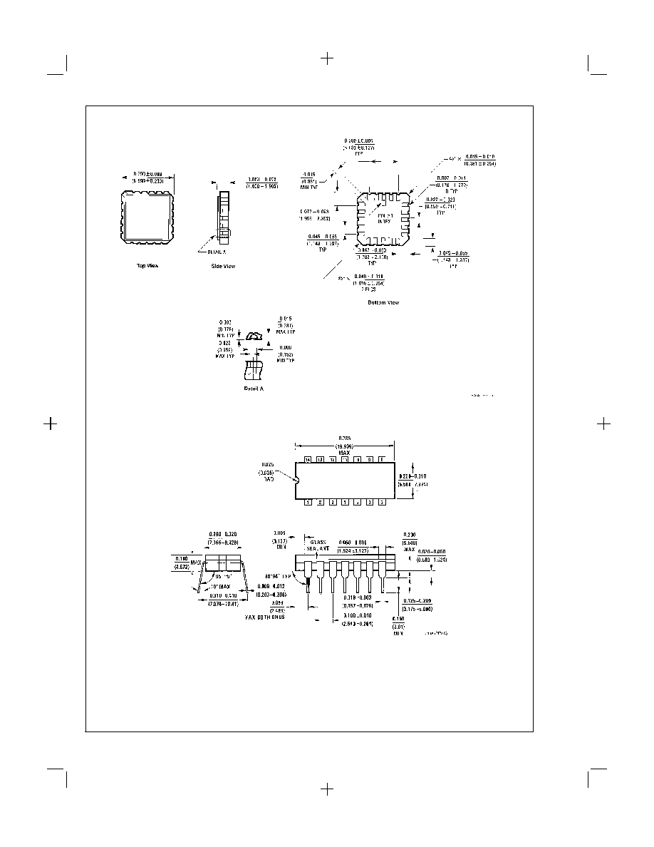
Physical Dimensions
inches (millimeters) unless otherwise noted
20-Lead Ceramic Leadless Chip Carrier (L)
NS Package Number E20A
14-Lead Ceramic Dual-In-Line Package (D)
NS Package Number J14A
5
www.national.com
PrintDate=1997/08/28 PrintTime=12:25:42 10193 ds009477 Rev. No. 1
cmserv
Proof
5
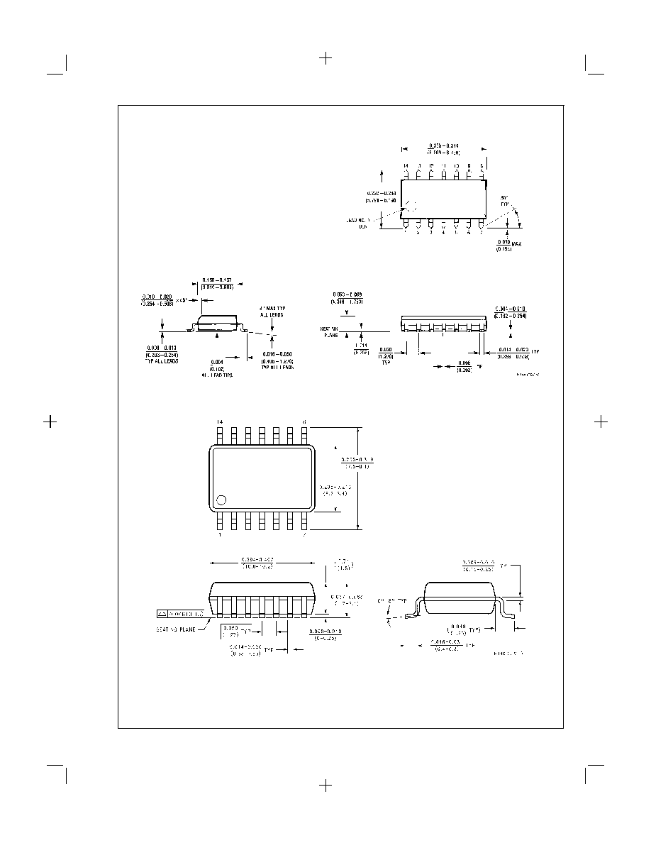
Physical Dimensions
inches (millimeters) unless otherwise noted (Continued)
14-Lead (0.150" Wide) Molded Small Outline Package, JEDEC (S)
NS Package Number M14A
14-Lead (0.300" Wide) Molded Small Outline Package, EIAJ (SJ)
NS Package Number M14D
PrintDate=1997/08/28 PrintTime=12:25:43 10193 ds009477 Rev. No. 1
cmserv
Proof
6
www.national.com
6

Physical Dimensions
inches (millimeters) unless otherwise noted (Continued)
14-Lead (0.300" Wide) (Molded Dual-In-Line Package (P)
NS Package Number N14A
14-Lead Ceramic Flatpak (F)
NS Package Number W14B
7
www.national.com
PrintDate=1997/08/28 PrintTime=12:25:43 10193 ds009477 Rev. No. 1
cmserv
Proof
7
LIFE SUPPORT POLICY
NATIONAL'S PRODUCTS ARE NOT AUTHORIZED FOR USE AS CRITICAL COMPONENTS IN LIFE SUPPORT DE-
VICES OR SYSTEMS WITHOUT THE EXPRESS WRITTEN APPROVAL OF THE PRESIDENT OF NATIONAL SEMI-
CONDUCTOR CORPORATION. As used herein:
1. Life support devices or systems are devices or sys-
tems which, (a) are intended for surgical implant into
the body, or (b) support or sustain life, and whose fail-
ure to perform when properly used in accordance
with instructions for use provided in the labeling, can
be reasonably expected to result in a significant injury
to the user.
2. A critical component in any component of a life support
device or system whose failure to perform can be rea-
sonably expected to cause the failure of the life support
device or system, or to affect its safety or effectiveness.
National Semiconductor
Corporation
Americas
Tel: 1-800-272-9959
Fax: 1-800-737-7018
Email: support@nsc.com
www.national.com
National Semiconductor
Europe
Fax: +49 (0) 1 80-530 85 86
Email: europe.support@nsc.com
Deutsch Tel: +49 (0) 1 80-530 85 85
English
Tel: +49 (0) 1 80-532 78 32
FranÁais Tel: +49 (0) 1 80-532 93 58
Italiano
Tel: +49 (0) 1 80-534 16 80
National Semiconductor
Hong Kong Ltd.
13th Floor, Straight Block,
Ocean Centre, 5 Canton Rd.
Tsimshatsui, Kowloon
Hong Kong
Tel: (852) 2737-1600
Fax: (852) 2736-9960
National Semiconductor
Japan Ltd.
Tel: 81-3-5620-6175
Fax: 81-3-5620-6179
54F/74F132
Quad
2-Input
NAND
Schmitt
T
rigger
8
PrintDate=1997/08/28 PrintTime=12:25:44 10193 ds009477 Rev. No. 1
cmserv
Proof
8
National does not assume any responsibility for use of any circuitry described, no circuit patent licenses are implied and National reserves the right at any time without notice to change said circuitry and specifications.