� 2000 National Semiconductor Corporation
www.national.com
GeodeTM
C
S
9210
G
raphics
Companion
D
STN
C
ont
r
o
l
l
er
April 2000
GeodeTM CS9210 Graphics Companion
DSTN Controller
General Description
The CS9210 graphics companion is suitable for systems
that use either the GXLV or GXm processor along with the
CS5530 I/O companion; all members of the National
Semiconductor
�
GeodeTM
family
of
products.
The
CS9210 converts the digital RGB output stream to the dig-
ital graphics input stream required by most industry stan-
dard DSTN color flat panel LCDs. It can drive all standard
DSTN flat panels up to a 1024x768 resolution. The sys-
tem connection example shows how the CS9210 inter-
faces with the rest of the system components.
Features
18-bit color support for digital pixel input
65 MHz pixel clock operation supports up to 1024x768
panels
Simultaneous CRT and DSTN display with up to 75 Hz
refresh rate
2X display refresh modes, up to 120 Hz
Supports most SVGA DSTN panels and the VESA
FPDI (Flat Panel Display Interface) Revision 1.0
Specification
TFT panel support provided by use of one connector;
allows a pass-through mode for the digital pixel input
Programmable frame rate modulation (FRM), up to 32
levels
Programmable dither, up to 16 levels
Supports EDO memory, 16-bit interface
Configuration via a serial programming interface
Low-power, 3.3V operation
144-pin LQFP (Low-profile Quad Flat Pack)
GeodeTM CS9210 System Connection Example
DRAM Data
Addr Control
13
16
LCD Power
3
Control
Clocks
3
16
Panel Data
DSTN
Pixel Port
24
Pixel Data
LCD
18
GeodeTM
GXm
GeodeTM
GeodeTM
CS9210
Graphics
CS5530
DRAM-B
256Kx16 bit
or
GXLV
Processor
DRAM-A
256Kx16 bit
Addr Control
13
DRAM Data
16
4
Serial
Configuration
I/O
Companion
Companion
Video Port (YUV)
National Semiconductor is a registered trademark of National Semiconductor Corporation.
Geode is a trademark of National Semiconductor Corporation.
For a complete listing of National Semiconductor trademarks, please visit www.national.com/trademarks.

www.national.com
2
Revision 3.2
Table of Contents
GeodeTM
C
S9210
1.0
Architecture Overview . . . . . . . . . . . . . . . . . . . . . . . . . . . . . . . . . . . . . . . . . . . . . . 3
2.0
Signal Definitions . . . . . . . . . . . . . . . . . . . . . . . . . . . . . . . . . . . . . . . . . . . . . . . . . . 4
2.1
PIN ASSIGNMENTS . . . . . . . . . . . . . . . . . . . . . . . . . . . . . . . . . . . . . . . . . . . . . . . . . . . . . . . 4
2.2
SIGNAL DESCRIPTIONS . . . . . . . . . . . . . . . . . . . . . . . . . . . . . . . . . . . . . . . . . . . . . . . . . . . 8
2.2.1
Pixel Port Interface Signals . . . . . . . . . . . . . . . . . . . . . . . . . . . . . . . . . . . . . . . . . . . 8
2.2.2
Serial Interface Signals . . . . . . . . . . . . . . . . . . . . . . . . . . . . . . . . . . . . . . . . . . . . . . 9
2.2.3
Flat Panel Interface Signals . . . . . . . . . . . . . . . . . . . . . . . . . . . . . . . . . . . . . . . . . . . 9
2.2.4
Memory Interface Signals . . . . . . . . . . . . . . . . . . . . . . . . . . . . . . . . . . . . . . . . . . . 10
2.2.5
Reset and Internal Test Pins . . . . . . . . . . . . . . . . . . . . . . . . . . . . . . . . . . . . . . . . . 11
2.2.6
Power and Ground Pins . . . . . . . . . . . . . . . . . . . . . . . . . . . . . . . . . . . . . . . . . . . . . 11
3.0
Functional Description . . . . . . . . . . . . . . . . . . . . . . . . . . . . . . . . . . . . . . . . . . . . 12
3.1
MODE SELECTION . . . . . . . . . . . . . . . . . . . . . . . . . . . . . . . . . . . . . . . . . . . . . . . . . . . . . . . 12
3.2
2X REFRESH MODE . . . . . . . . . . . . . . . . . . . . . . . . . . . . . . . . . . . . . . . . . . . . . . . . . . . . . . 14
3.3
TIMING SIGNALS AND PANEL CLOCK . . . . . . . . . . . . . . . . . . . . . . . . . . . . . . . . . . . . . . . 15
3.4
SIMULTANEOUS DISPLAY . . . . . . . . . . . . . . . . . . . . . . . . . . . . . . . . . . . . . . . . . . . . . . . . . 15
3.5
MAXIMUM FREQUENCY . . . . . . . . . . . . . . . . . . . . . . . . . . . . . . . . . . . . . . . . . . . . . . . . . . . 16
3.6
RESET PROCEDURES . . . . . . . . . . . . . . . . . . . . . . . . . . . . . . . . . . . . . . . . . . . . . . . . . . . . 16
3.7
SERIAL INTERFACE . . . . . . . . . . . . . . . . . . . . . . . . . . . . . . . . . . . . . . . . . . . . . . . . . . . . . . 16
3.8
COLOR GENERATION . . . . . . . . . . . . . . . . . . . . . . . . . . . . . . . . . . . . . . . . . . . . . . . . . . . . 18
3.8.1
Frame Rate Modulation (FRM) . . . . . . . . . . . . . . . . . . . . . . . . . . . . . . . . . . . . . . . . 18
3.8.1.1
Choosing FRM Sequences . . . . . . . . . . . . . . . . . . . . . . . . . . . . . . . . . . . . . . . . . . 18
3.8.1.2
Removal of Flickering . . . . . . . . . . . . . . . . . . . . . . . . . . . . . . . . . . . . . . . . . . . . . . 20
3.8.2
Dithering . . . . . . . . . . . . . . . . . . . . . . . . . . . . . . . . . . . . . . . . . . . . . . . . . . . . . . . . . 20
3.8.2.1
N-Bit Dithering Schemes . . . . . . . . . . . . . . . . . . . . . . . . . . . . . . . . . . . . . . . . . . . . 21
3.8.3
Combining FRM and Dithering . . . . . . . . . . . . . . . . . . . . . . . . . . . . . . . . . . . . . . . . 22
3.8.3.1
Modified FRM and Dithering . . . . . . . . . . . . . . . . . . . . . . . . . . . . . . . . . . . . . . . . . 22
3.9
PROGRAMMING THE FRM AND DITHER MEMORIES . . . . . . . . . . . . . . . . . . . . . . . . . . . 22
3.9.1
Addressing the FRM Memories . . . . . . . . . . . . . . . . . . . . . . . . . . . . . . . . . . . . . . . 22
3.9.2
Addressing the Dithering Memories . . . . . . . . . . . . . . . . . . . . . . . . . . . . . . . . . . . . 23
4.0
Register Descriptions . . . . . . . . . . . . . . . . . . . . . . . . . . . . . . . . . . . . . . . . . . . . . 24
5.0
Electrical Specifications . . . . . . . . . . . . . . . . . . . . . . . . . . . . . . . . . . . . . . . . . . . 30
5.1
ABSOLUTE MAXIMUM RATINGS . . . . . . . . . . . . . . . . . . . . . . . . . . . . . . . . . . . . . . . . . . . . 30
5.2
RECOMMENDED OPERATING CONDITIONS . . . . . . . . . . . . . . . . . . . . . . . . . . . . . . . . . . 30
5.3
DC CHARACTERISTICS
. . . . . . . . . . . . . . . . . . . . . . . . . . . . . . . . . . . . . . . . . . . . . . . . . . 31
5.4
AC CHARACTERISTICS . . . . . . . . . . . . . . . . . . . . . . . . . . . . . . . . . . . . . . . . . . . . . . . . . . . 32
5.4.1
Pixel Port Timing . . . . . . . . . . . . . . . . . . . . . . . . . . . . . . . . . . . . . . . . . . . . . . . . . . 33
5.4.2
Serial Interface Timing . . . . . . . . . . . . . . . . . . . . . . . . . . . . . . . . . . . . . . . . . . . . . . 34
5.4.3
Flat Panel Timing . . . . . . . . . . . . . . . . . . . . . . . . . . . . . . . . . . . . . . . . . . . . . . . . . . 35
5.4.4
Memory Interface Timing
. . . . . . . . . . . . . . . . . . . . . . . . . . . . . . . . . . . . . . . . . . . 36
6.0
Mechanical Package Outline . . . . . . . . . . . . . . . . . . . . . . . . . . . . . . . . . . . . . . . 37
Appendix A
Support Documentation . . . . . . . . . . . . . . . . . . . . . . . . . . . . . . . . . . . . 38
A.1
REVISION HISTORY . . . . . . . . . . . . . . . . . . . . . . . . . . . . . . . . . . . . . . . . . . . . . . . . . . . . . . 38
www.national.com
4
Revision 3.2
GeodeTM
C
S9210
2.0
Signal Definitions
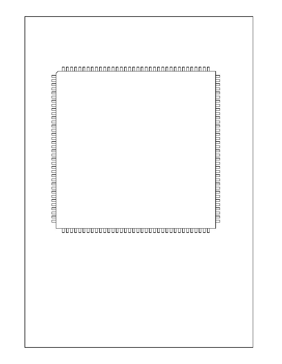
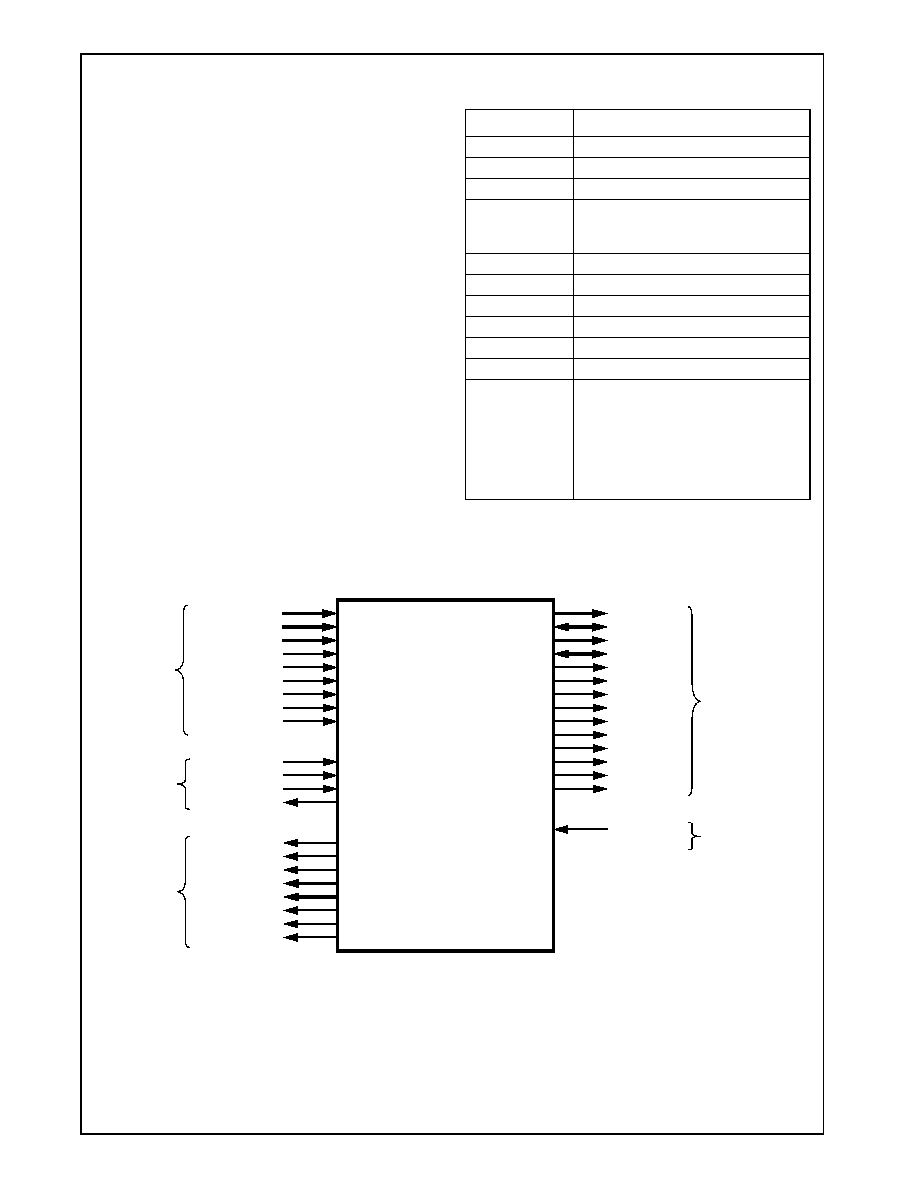
This section defines the signals and external interface of
the Geode CS9210. Figure 2-1 shows the pins organized
by their functional groupings (internal test and electrical
pins are not shown).
2.1
PIN ASSIGNMENTS
The tables in this section use several common abbrevia-
tions. Table 2-1 lists the mnemonics and their meanings.
Figure 2-2 shows the pin assignment for the CS9210 with
Tables 2-2 and 2-3 listing the pin assignments sorted by
pin number and alphabetically by signal name, respec-
tively.
In Section 2.2 "Signal Descriptions" a description of each
signal within its associated functional group is provided.
Figure 2-1. CS9210 Signal Groups
Table 2-1. Pin Type Definitions
Mnemonic
Definition
I
Standard input pin.
I/O
Bidirectional pin.
O
Totem-pole output.
OD
Open-drain output structure that
allows multiple devices to share the
pin in a wired-OR configuration
PU
Pull-up resistor
PD
Pull-down resistor
smt
Schmitt Trigger
t/s
Tri-state signal
VDD (PWR)
Power pin.
VSS (GND)
Ground pin
#
The "#" symbol at the end of a signal
name indicates that the active or
asserted state occurs when the signal
is at a low voltage level. When "#" is
not present after the signal name, the
signal is asserted when at a high volt-
age level.
RED[5:0]
GREEN[5:0]
BLUE[5:0]
ENA_DISP
ENA_VDDIN
ENA_LCDIN
DOTCLK
FP_HSYNC
FP_VSYNC
SCLK
SDIN
SCS
SDO
LP
SHFCLK
FLM
UD[11:0]
LD[11:0]
DISPOFF#
FP_VDDEN
FP_VCONEN
MA_A[9:0]
MD_A[15:0]
MA_B[9:0]
MD_B[15:0]
OEA#
OEB#
RASA#
RASB#
LCASA#
UCASA#
LCASB#
UCASB#
RESET#
Memory
Interface
Reset
Interface
Flat Panel
Interface
Pixel Port
Interface
GeodeTM CS9210
Graphics
Serial
Interface
WEA#
WEB#
Companion