Äîêóìåíòàöèÿ è îïèñàíèÿ www.docs.chipfind.ru
LM3743
N-Channel FET Synchronous Buck Controller for Low
Output Voltages
General Description
The LM3743 is a voltage mode PWM buck controller which
implements synchronous rectification. It provides a low cost,
fault tolerant, and efficient point of load solution. To reduce
component count several parameters are fixed, such as
switching frequency and the short circuit protection level. For
example the LM3743 has an operating switching frequency
of 300 kHz or 1 MHz and a fixed 500 mV high side current
limit for switch node short-circuit protection. LM3743 is a
very fault tolerant IC with switch node short-circuit, output
undervoltage protection, and the ability to self recover after
the removal of the fault. It avoids the need to over design
components due to thermal runaway during a fault condition,
thus resulting in a lower cost solution. It employs a propri-
etary monotonic glitch free pre-bias start-up method suited
for FPGAs and ASIC logic devices. A 0.8V internal reference
with
±
1.75% accuracy is ideal for sub-volt conversion. An
external programmable soft-start allows for tracking and tim-
ing flexibility. The driver features 1.6
of pull-up resistance
and 1
of pull-down drive resistance for high power density
and very efficient power processing.
Features
n
Input voltage from 3.0V to 5.5V
n
Output voltage adjustable down to 0.8V
n
Reference accuracy:
±
1.75%, over full temperature and
input voltage range
n
Low-side sensing programmable current limit
n
Fixed high-side sensing for supplemental short-circuit
protection
n
Undervoltage protection
n
Hiccup mode protection eliminates thermal runaway
during fault conditions
n
Externally programmable soft-start with tracking
capability
n
Switching frequency options of 1 MHz or 300 kHz
n
Pre-bias start-up capability
n
MSOP-10 package
Applications
n
ASIC/FPGA/DSP core power
n
Broadband Communications
n
Multi-media Set Top Boxes
n
Networking Equipment
n
Printers/Scanners
n
Servers
n
Low Voltage Distributed Power
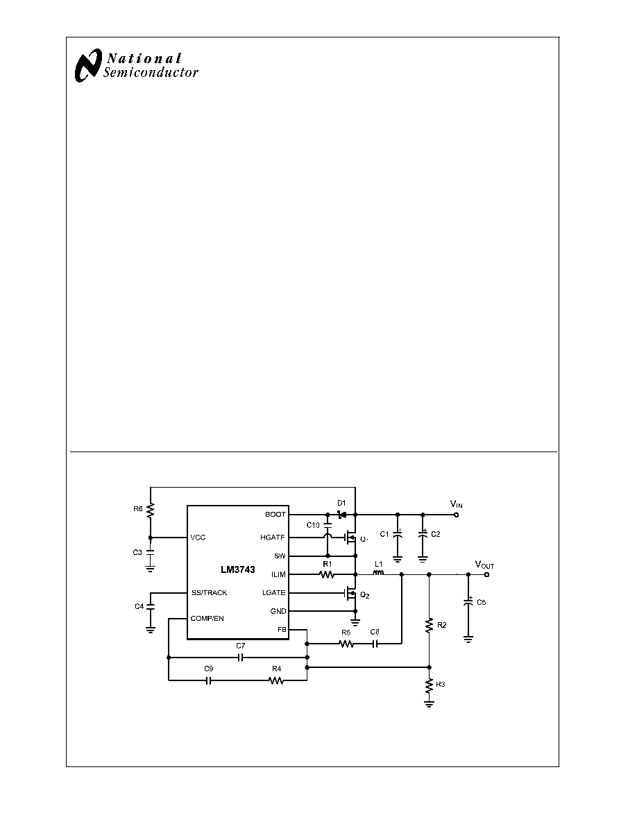
Typical Application
20177401
September 2006
LM3743
N-Channel
FET
Synchronous
Buck
Controller
for
Low
Output
V
oltages
© 2006 National Semiconductor Corporation
DS201774
www.national.com
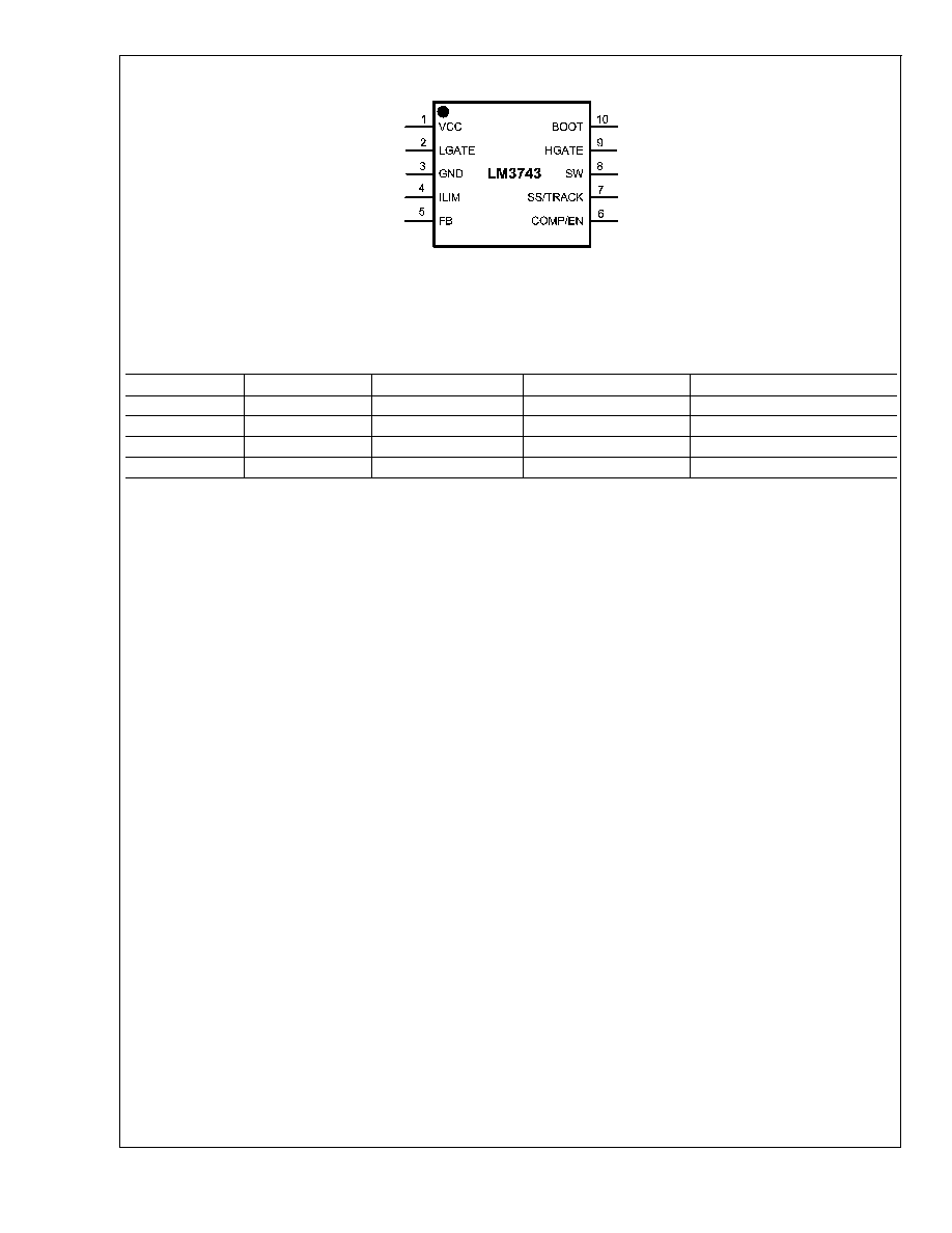
Connection Diagram
20177402
10-Lead Plastic MSOP
NS Package Number MUB10A
Top View
Ordering Information
Order Number
Frequency Option
Top Mark
NSC Package Drawing
Supplied As
LM3743MM-300
300 kHz
SKPB
MUB10A
1000 units in Tape and Reel
LM3743MMX-300
300 kHz
SKPB
MUB10A
3500 units in Tape and Reel
LM3743MM-1000
1 MHz
SKNB
MUB10A
1000 units in Tape and Reel
LM3743MMX-1000
1 MHz
SKNB
MUB10A
3500 units in Tape and Reel
Pin Descriptions
VCC (Pin 1) Supply rail for the controller section of the IC. A
minimum capacitance of 1 µF, preferably a multi-layer ce-
ramic capacitor type (MLCC), must be connected as close
as possible to the V
CC
and GND pin and a 1 to 4.99
resistance must be connected in series from the supply rail
to the Vcc pin. See VCC FILTERING in the Design Consid-
eration section for further details.
LGATE (Pin 2) Gate drive for the low-side N-channel MOS-
FET. This signal is interlocked with HGATE to avoid a shoot-
through problem.
GND (Pin 3) Power ground (PGND) and signal ground
(SGND). Connect the bottom feedback resistor between this
pin and the feedback pin.
ILIM (Pin 4) Low side current limit threshold setting pin. This
pin sources a fixed 50 µA current. A resistor of appropriate
value should be connected between this pin and the drain of
the low-side N-FET.
FB (Pin 5) Feedback pin. This is the inverting input of the
error amplifier used for sensing the output voltage and com-
pensating the control loop.
COMP/EN (Pin 6) Output of the error amplifier and enable
pin. The voltage level on this pin is compared with an inter-
nally generated ramp signal to determine the duty cycle. This
pin is necessary for compensating the control loop. Forcing
this pin to ground will shut down the IC.
SS/TRACK (Pin 7) Soft-start and tracking pin. This pin is
connected to the non-inverting input of the error amplifier
during initial soft-start, or any time the voltage is below the
reference. To track the rising ramp of another power supply's
output, connect a resistor divider from the output of that
supply to this pin as described in Application Information.
SW (Pin 8) Switch pin. The lower rail of the high-side N-FET
driver. Also used for the high side current limit sensing.
HGATE (Pin 9) Gate drive for the high-side N-channel MOS-
FET. This signal is interlocked with LGATE to avoid a shoot-
through problem.
BOOT (Pin 10) Supply rail for the N-channel MOSFET high
gate drive. The voltage should be at least one gate threshold
above the regulator input voltage to properly turn on the
high-side N-FET. See MOSFET Gate Drivers in the Applica-
tion Information section for more details on how to select
MOSFETs.
LM3743
www.national.com
2
Absolute Maximum Ratings
(Note 1)
If Military/Aerospace specified devices are required,
please contact the National Semiconductor Sales Office/
Distributors for availability and specifications.
V
CC
-0.3V to 6V
SW to GND
-0.3V to 6V
Boot to GND
-0.3V to 12V
Boot to SW
-0.3V to 6V
SS/TRACK, ILIM,
COMP/EN,FB to GND
-0.3V to V
CC
Junction Temperature
150°C
Storage Temperature
-65°C to 150°C
Soldering Information
Lead Temperature (soldering, 10sec)
260°C
Infrared or Convection (20sec)
235°C
ESD Rating (Note 3)
+ / 2 kV
Operating Ratings
Supply Voltage Range, V
CC
(Note 2)
3.0V to 5.5V
Junction Temperature Range (T
J
)
-40°C to +125°C
Electrical Characteristics
V
CC
= 3.3V, COMP/EN floating unless otherwise indicated in the conditions col-
umn. Limits in standard type are for T
J
= 25°C only; limits in boldface type apply over the junction temperature (T
J
) range of
-40°C to +125°C. Minimum and Maximum limits are guaranteed through test, design, or statistical correlation. Typical values
represent the most likely parametric norm at T
J
= 25°C, and are provided for reference purposes only.
Symbol
Parameter
Conditions
Min
Typ
Max
Units
SYSTEM PARAMETERS
V
FB
FB pin voltage in regulation
3.0V
V
CC
5.5V
0.786
0.8
0.814
V
V
UVLO
UVLO thresholds
Input voltage rising
2.84
3.0
V
Input voltage falling
2.45
2.66
I
VCC
Operating V
CC
current
f
SW
= 300 kHz, LM3743-300
1.5
2.5
mA
Operating V
CC
current
f
SW
= 1 MHz, LM3743-1000
1.8
3.0
mA
Shutdown V
CC
current
COMP/EN = 0V
6
50
µA
I
SS/TRACK
SS/TRACK pin source current
V
SS/TRACK
= 0V
8
10.2
12.5
µA
I
ILIM
ILIM pin source current
V
ILIM
= 0V
42.5
50
57.5
µA
V
ILIM
Current Limit Trip Level
25
0
25
mV
I
COMP/EN
COMP/EN pin pull-up current
V
COMP/EN
= 0V
4
µA
V
HS-CLIM
High-side current limit threshold
Measured at V
CC
pin with respect to
SW
500
mV
ERROR AMPLIFER
GBW
Error Amplifier Unity Gain Bandwidth
30
MHz
G
Error Amplifier DC Gain
90
dB
SR
Error Amplifier Slew Rate
6
V/ms
I
FB
FB pin Bias Current
10
200
nA
I
EAO
EAO pin sourcing/sinking current
capability
V
COMP/EN
= 1.5, V
FB
= 0.75V
1.7
mA
V
COMP/EN
= 1.5, V
FB
= 0.85V
-1
GATE DRIVE
I
SHDN-BOOT
BOOT Pin Shutdown Current
V
BOOT
-V
SW
= 3.3V, V
COMP/EN
= 0V
25
50
µA
R
HG-UP
High Side MOSFET Driver Pull-up ON
resistance
V
BOOT
-V
SW
= 3.3V, I
HGATE
= 350mA
(sourcing)
1.6
R
HG-DN
High Side MOSFET Driver Pull-down ON
resistance
V
BOOT
-V
SW
= 3.3V, I
HGATE
= 350mA
(sinking)
1
R
LG-UP
Low Side MOSFET Driver Pull-up ON
resistance
V
CC
= 3.3V, I
LGATE
= 350mA
(sourcing)
1.6
R
LG-DN
Low Side MOSFET Driver Pull-down ON
resistance
V
CC
= 3.3V, I
LGATE
= 350mA (sinking)
1
OSCILLATOR
f
SW
Oscillator Frequency
3.0V
V
CC
5.5V, LM3743-300
255
300
345
kHz
3.0V
V
CC
5.5V, LM3743-1000
850
1000
1150
D
MAX
Max Duty Cycle
f
SW
= 300 kHz, LM3743-300
85
91
%
f
SW
= 1 MHz, LM3743-1000
69
76
LM3743
www.national.com
3
Electrical Characteristics
V
CC
= 3.3V, COMP/EN floating unless otherwise indicated in the conditions
column. Limits in standard type are for T
J
= 25°C only; limits in boldface type apply over the junction temperature (T
J
) range of
-40°C to +125°C. Minimum and Maximum limits are guaranteed through test, design, or statistical correlation. Typical values
represent the most likely parametric norm at T
J
= 25°C, and are provided for reference purposes only. (Continued)
Symbol
Parameter
Conditions
Min
Typ
Max
Units
V
RAMP
PWM Ramp Amplitude
1.0
V
LOGIC INPUTS AND OUTPUTS
V
COMP/EN-HI
COMP/EN pin logic high trip-point
0.65
0.9
V
V
COMP/EN-LO
COMP/EN pin logic low trip-point
0.1
0.45
V
HICCUP MODE
N
LSCYCLES
Low-side sensing cycles before hiccup
mode
15
Cycles
N
LSRESET
Low-side sensing cycles reset without
activating current limit
32
Cycles
V
UVP
Under Voltage Protection comparator
threshold
400
mV
t
GLICH-UVP
Under Voltage Protection fault time before
hiccup mode
7
µs
t
HICCUP
Hiccup timeout
5.5
ms
t
SS
Soft-start time coming out of hiccup mode
3.6
ms
THERMAL RESISTANCE
JA
Junction to Ambient Thermal Resistance
235
°C/W
Note 1: Absolute maximum ratings indicate limits beyond which damage to the device may occur. Operating ratings indicate conditions for which the device
operates correctly. Operating Ratings do not imply guaranteed performance limits.
Note 2: Practical lower limit of V
CC
depends on selection of the external MOSFET. See the MOSFET GATE DRIVERS section under Application Information for
further details.
Note 3: ESD using the human body model which is a 100 pF capacitor discharged through a 1.5 k
resistor into each pin. Test method is per JESD22A114.
LM3743
www.national.com
4
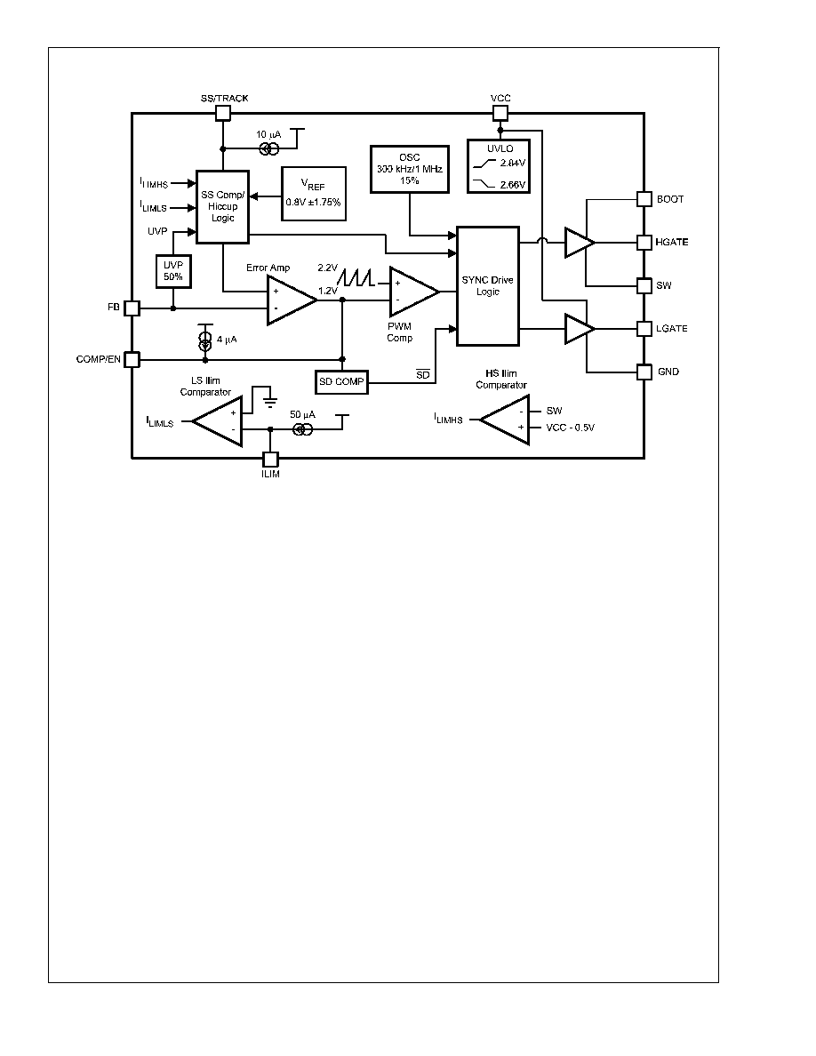
Block Diagram
20177403
LM3743
www.national.com
5
Document Outline