 | ÐлекÑÑоннÑй компоненÑ: LM4832MT | СкаÑаÑÑ:  PDF PDF  ZIP ZIP |
LM4832 Boomer ® Audio Power Amplifier Series Digitally Controlled Tone and Volume Circuit with Stereo Audio Power Amplifier, Microphone Preamp Stage and National 3D Sound
LM4832
Digitally Controlled Tone and Volume Circuit with Stereo
Audio Power Amplifier, Microphone Preamp Stage and
National 3D Sound
General Description
The LM4832 is a monolithic integrated circuit that provides
volume and tone (bass and treble) controls as well as a
stereo audio power amplifier capable of producing 250 mW
(typ) into 8
or 90 mW (typ) into 32 with less than 1.0%
THD. In addition, a two input microphone preamp stage, with
volume control, capable of driving a 1 k
load is imple-
mented on chip.
The LM4832 also features National's 3D Sound circuitry
which can be externally adjusted via a simple RC network.
For maximum system flexibility, the LM4832 has an exter-
nally controlled, low-power consumption shutdown mode,
and an independent mute for power and microphone ampli-
fiers .
Boomer
®
audio integrated circuits were designed specifically
to provide high quality audio while requiring few external
components. Since the LM4832 incorporates tone and vol-
ume controls, a stereo audio power amplifier and a micro-
phone preamp stage, it is optimally suited to multimedia
monitors and desktop computer applications.
Key Specifications
n
Output Power at 10% into 8
350mW (typ)
n
Output Power at 10% into 32
100mW (typ)
n
THD+N at 75mW into 32
at 1kHz
0.5% (max)
n
Microphone Input Referred Noise
7µV (typ)
n
Supply Current
13mA (typ)
n
Shutdown Current
4µA (typ)
Features
n
Independent Left and Right Output Volume Controls
n
Treble and Bass Control
n
National 3D Sound
n
I
2
C Compatible Interface
n
Two Microphone Inputs with Selector
n
Software Controlled Shutdown Function
Applications
n
Multimedia Monitors
n
Portable and Desktop Computers
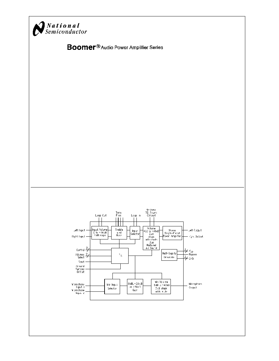
Block Diagram
Boomer
®
is a registered trademark of National Semiconductor Corporation.
10001401
FIGURE 1. LM4832 Block Diagram
October 2002
LM4832
Digitally
Controlled
T
one
and
V
olume
Circuit
with
Stereo
Audio
Power
Amplifier
,
Microphone
Preamp
Stage
and
National
3D
Sound
© 2002 National Semiconductor Corporation
DS100014
www.national.com
Absolute Maximum Ratings
(Note 2)
If Military/Aerospace specified devices are required,
please contact the National Semiconductor Sales Office/
Distributors for availability and specifications.
Supply Voltage
6.0V
Storage Temperature
-65°C to +150°C
Input Voltage
-0.3V to V
DD
+0.3V
Power Dissipation (Note 3)
Internally limited
ESD Susceptibility (Note 4)
2000V
ESD Susceptibility (Note 5)
250V
Junction Temperature
150°C
Soldering Information
Small Outline Package
Vapor Phase (60 sec.)
215°C
Infrared (15 sec.)
220°C
See AN-450 'Surface Mounting and their Effects on
Product Reliability' for other methods of soldering surface
mount devices.
JC
(typ) -- N28B
21°C/W
JA
(typ) -- N28B
62°C/W
JC
(typ) -- M28B
15°C/W
JA
(typ) -- M28B
69°C/W
JC
(typ) -- MTC28
20°C/W
JA
(typ) -- MTC28
80°C/W
Operating Ratings
Temperature Range
T
MIN
T
A
T
MAX
-40°C
T
A
85°C
Supply Voltage
4.5
V
DD
5.5V
Electrical Characteristics for Entire IC
(Notes 1, 2)
The following specifications apply for V
DD
= 5V unless otherwise noted. Limits apply for T
A
= 25°C.
Symbol
Parameter
Conditions
LM4832
Units
(Limits)
Typical
(Note 6)
Limit
(Note 7)
V
DD
Supply Voltage
V
IN
= 0V, I
O
= 0A
4.5
V (min)
5.5
V (max)
I
DD
Quiescent Power Supply Current
13
21
mA (max)
I
SD
Shutdown Current
2.5
9
µA (max)
INPUT ATTENUATORS
A
R
Attenuator Range
Attenuation at 0 dB Setting
Attenuation at -14 dB Setting
1
-15
dB (max)
dB (min)
A
S
Step Size
0 dB to -14 dB
2
dB
Gain Step Size Error
0.1
dB (max)
E
T
Channel to Channel Tracking Error
0.15
dB (max)
BASS CONTROL
A
R
Bass Control Range
f = 100 Hz, V
IN
= 0.25V
±
12
-14
dB (min)
14
dB (max)
A
S
Bass Step Size
2
dB
E
SE
Bass Step Size Error
0.5
dB (max)
E
T
Bass Tracking Error
0.15
dB (max)
TREBLE CONTROL
A
R
Treble Control Range
f
IN
= 10 kHz, V
IN
= 0.25V
±
12
-13
dB (min)
13
dB (max)
A
S
Treble Step Size
2
dB
E
SE
Treble Step Size Error
0.1
dB (max)
E
T
Treble Tracking Error
0.15
dB (max)
OUTPUT ATTENUATORS
A
R
Attenuator Range
Gain at +20 dB Setting
Attenuation at -40 dB Setting
+20 dB to -40 dB
21
dB (max)
-42
dB (min)
A
S
Step Size
2
dB
Step Size Error
0.1
dB (max)
E
T
Channel to Channel Tracking Error
0.1
dB (max)
LM4832
www.national.com
2

Electrical Characteristics for Entire IC
(Notes 1, 2) (Continued)
The following specifications apply for V
DD
= 5V unless otherwise noted. Limits apply for T
A
= 25°C.
Symbol
Parameter
Conditions
LM4832
Units
(Limits)
Typical
(Note 6)
Limit
(Note 7)
AUDIO PATH
V
OS
Output Offset Voltage
V
IN
= 0V
3
50
mV (max)
P
O
Output Power
THD = 1.0% (max), f = 1 kHz, All
controls at 0dB
R
L
= 8
250
mW (min)
R
L
= 32
95
75
mW (min)
THD+N
Total Harmonic Distortion+Noise
All Controls at 0 dB, THD = 10%, f = 1
kHz
R
L
= 8
350
mW
P
O
= 200 mW, R
L
= 8
0.15
%
P
O
= 75 mW, R
L
= 32
0.11
%
V
O
= 1 Vrms, R
L
= 10
0.08
%
PSRR
Power Supply Rejection Ratio
C
B
= 1 µF, f = 100 Hz, V
RIPPLE
= 100
mVrms, All Controls at 0 dB Setting
45
dB
A
M
Mute Attenuation
f = 1 kHz, V
IN
= 1V
-75
dB
X
TALK
Cross Talk
P
O
= 200 mW, R
L
= 8
,
All controls at 0 dB setting,
f = 1 kHz
Left to Right
-85
dB
Right to Left
-72
dB
MICROPHONE PREAMP AND VOLUME CONTROL
A
V
Preamp Gain
0 dB Gain
0
-1, 1
dB
+20 dB Gain
20
19, 21
dB
+30 dB Gain
30
29, 31
dB
A
R
Attenuator Range
Gain at +18 dB Setting
20
dB (max)
Attenuation at -42 dB Setting
-43
dB (min)
A
S
Step Size
0 dB to -42 dB
3
dB
Step Size Error
0.4
dB (max)
V
SWING
Output Voltage Swing
f = 1 kHz, THD
<
1.0%, R
L
= 1 k
1.7
V
rms
E
NO
Input Referred Noise
A-Weighted, Attenuator at 0 dB
7
µV (min)
PSRR
Power Supply Rejection Ratio
f = 100 Hz, V
RIPPLE
= 100 mVrms,
C
B
= 1 µF
35
dB
A
M
Mute Attenuation
-90
dB
X
TALK
Cross Talk
Power Amp P
O
= 200 mW, f = 1 kHz
-90
dB
THD+N
Total Harmonic Distortion Plus Noise
All controls at 0 dB, f = 1 kHz, V
O
= 1V
0 dB Setting
0.03
%
+20 dB Gain
0.03
%
+30 dB Gain
0.04
%
I
2
C BUS TIMING
f
MAX
Maximum Bus Frequency
400
kHz
T
START:HOLD
Start Signal: Hold Time before
Clock/Data Transitions
0.6
µs
T
D;SETUP
Data Setup Time
0.1
µs
T
C;HIGH
Minimum High Clock Duration
0.6
µs
T
C;LOW
Minimum Low Clock Duration
1.3
µs
T
STOP;SETUP
Stop Signal: Setup Time before
Clock/Data Transitions
0.6
µs
LM4832
www.national.com
3
Electrical Characteristics for Entire IC
(Notes 1, 2) (Continued)
The following specifications apply for V
DD
= 5V unless otherwise noted. Limits apply for T
A
= 25°C.
Symbol
Parameter
Conditions
LM4832
Units
(Limits)
Typical
(Note 6)
Limit
(Note 7)
I
2
C BUS INPUT AND OUTPUT
V
IL
Input Low Voltage
1.5
V (max)
V
IH
Input High Voltage
3
V (min)
I
IN
Input Current
0.15
µA
V
O
Output Voltage -- SDA Acknowledge
0.4
V (max)
V
OL
External Power Amp Disable Low
0.4
V (max)
V
OH
External Power Amp Disable High
4
V (min)
Note 1: All voltages are measured with respect to the ground pins, unless otherwise specified. All specifications are tested using the typical applicationas shown
in Figure 1.
Note 2: Absolute Maximum Ratings indicate limits beyond which damage to the device may occur. Operating Ratings indicate conditions for which the device is
functional, but do not guarantee specific performance limits. Electrical Characteristics state DC and AC electrical specifications under particular test conditions which
guarantee specific performance limits. This assumes that the device is within the Operating Ratings. Specifications are not guaranteed for parameters where no limit
is given, however, the typical value is a good indication of device performance.
Note 3: The maximum power dissipation must be derated at elevated temperatures and is dictated by T
JMAX
,
JA
, and the ambient temperature T
A
. The maximum
allowable power dissipation is P
DMAX
= (T
JMAX
- T
A
)/
JA
.For the LM4832, T
JMAX
= 150°C, and the typical junction-to-ambient thermal resistance, when board
mounted, is 69°C/W assuming the M28B package.
Note 4: Human body model, 100 pF discharged through a 1.5 k
resistor.
Note 5: Machine Model, 220 pF240 pF discharged through all pins.
Note 6: Typicals are measured at 25°C and represent the parametric norm.
Note 7: Limits are guaranteed that all parts are tested in production to meet the stated values.
LM4832
www.national.com
4
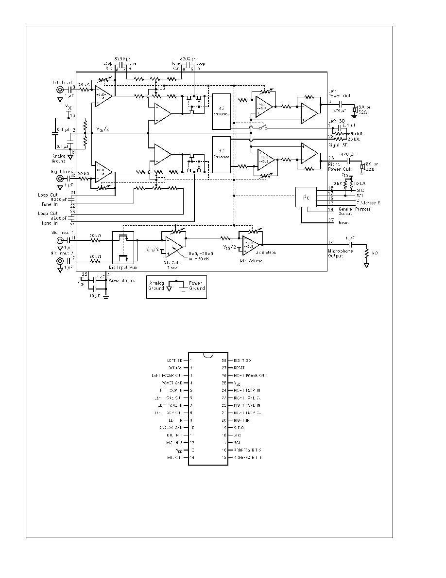
Typical Application Circuit
Connection Diagram
10001402
Top View
Order Number LM4832N, LM4832M
See NS Package Number N28B for DIP
See NS Package Number M28B for SOIC
See NS Package Number MTC28 for TSSOP
10001403
FIGURE 2. Typical Application Circuit
LM4832
www.national.com
5
Document Outline