LM4921
Low Voltage I
2
S 16-Bit Stereo DAC with Stereo
Headphone Power Amplifiers and Volume Control
General Description
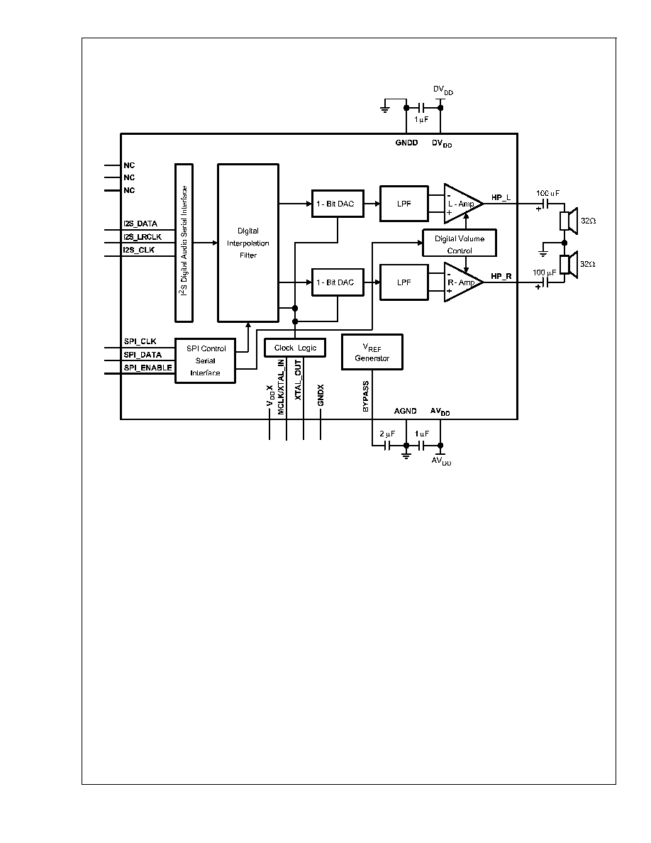
The LM4921 combines a 16-bit resolution stereo I
2
S input
digital-to-analog converter (DAC) with a stereo headphone
audio power amplifier. It is primarily designed for demanding
applications in mobile phones and other portable communi-
cation device applications. The LM4921 features an I
2
S
serial interface for the digital audio information and a 16-bit
SPI serial interface for internal register control and commu-
nication. With AV
DD
and DV
DD
= 3.0V
DC
and driving a 32
single-ended load to a 26mW
RMS
output level the distortion
(THD+N) of the LM4921 will be less than 0.5%. The LM4921
also features a programmable 32-step digital volume control
accessed through an SPI interface.
Boomer audio power amplifiers were designed specifically to
provide high quality output power with a minimal amount of
external components. It is, therefore, ideally suited for mo-
bile phone and other low voltage applications where minimal
power consumption is a primary requirement.
The LM4921 features a low-power consumption shutdown
mode, and also has an internal thermal shutdown protection
mechanism.
Key Specifications
j
PSRR at 217Hz, A/DV
DD
= 3V, (Fig. 1)
52dB (typ)
j
P
OUT
at AV
DD
= 3.0V, 32
<
0.05% THD
13mW (typ)
<
0.5% THD
26mW (typ)
j
Supply voltage range
DV
DD
2.6V to 5.0V
AV
DD
(Note 8)
2.6V to 5.5V
j
Shutdown current
1�A (typ)
Features
n
16-bit resolution stereo DAC
n
I
2
S digital audio data serial interface
n
SPI serial interface (control register)
n
Volume Control (32 steps; 1.5 dB increments)
n
Up to 50mW/channel stereo headphone amplifier
n
Zero Crossing Detection for Silent Attenuation Steps
n
2.6V
DC
to 5.0V
DC
digital supply voltage range
n
2.6V
DC
to 5.5V
DC
analog supply voltage range (Note 8)
n
Unity-gain stable headphone amplifiers
n
Available in the 20-bump microSMD package
Applications
n
Mobile phones
n
PDAs
n
Portable electronic devices
Boomer
�
is a registered trademark of National Semiconductor Corporation.
November 2004
LM4921
Low
V
oltage
I
2
S
16-Bit
Stereo
DAC
with
Stereo
Headphone
Power
Amplifiers
and
V
olume
Control
� 2004 National Semiconductor Corporation
DS200486
www.national.com

Connection Diagrams
LM4921 Pin Configuration
200486F8
Top View
20-Bump micro SMD
Order Number LM4921ITL, LM4921ITLX
See NS Package Number TLA20JKA
NC - No Connection
20-Bump micro SMD Marking
200486F9
X - Date Code
T - Die Traceability
G - Boomer Family
B9 - LM4921ITL
LM4921
www.national.com
3
LM4921 I/O Pin Descriptions
PIN # (ITL)
PIN NAME
PIN TYPE
Input-I, Output-O,
Power-P, No Connect-NC
PIN DESCRIPTION
B1
I2S_CLK
I/O
I2S Clock
C2
I2S_DATA
I
I2S data
B2
I2S_WS
I/O
I2S L/R word select
E3
SPI_CLK
I
SPI clcock
E4
SPI_DATA
I
SPI data
D3
SPI_ENABLE
I
SPI Enable
E2
MCLK/XTAL_IN
I
Master Clock / Xtal input
D2
XTAL_OUT
O
Xtal output
C4
BYPASS
I/O
Analog VDD/2 bypass capacitor connection
point
B4
AV
DD
P
Analog supply
A3
AGND
P
Analog Ground
C1
DV
DD
P
Digital Supply
A1
GNDD
P
Digital ground
D1
VDDX
P
XTAL Oscillator circuit supply
E1
GNDX
P
XTAL Oscillator circuit ground
B3
HP_L
O
HP left output
A4
HP_R
O
HP right output
A2
No Connect
O
Must let float
C3
No Connect
NC
NC
D4
No Connect
NC
NC
LM4921
www.national.com
4
Absolute Maximum Ratings
(Notes 1, 2)
If Military/Aerospace specified devices are required,
please contact the National Semiconductor Sales Office/
Distributors for availability and specifications.
Supply Voltage
6.0V
Storage Temperature
-65�C to +150�C
Input Voltage
-0.3V to V
DD
+ 0.3V
Power Dissipation (Note 3)
Internally Limited
ESD Susceptibility
Human body model (Note 4)
2000V
Machine model (Note 5)
200V
Junction Temperature
150�C
Thermal Resistance
JA
60�C/W
Operating Ratings
Temperature Range
T
MIN
T
A
T
MAX
-40�C
T
A
85�C
Supply Voltage
DV
DD
2.6V
DV
DD
5.0V
AV
DD
2.6V
AV
DD
5.5V
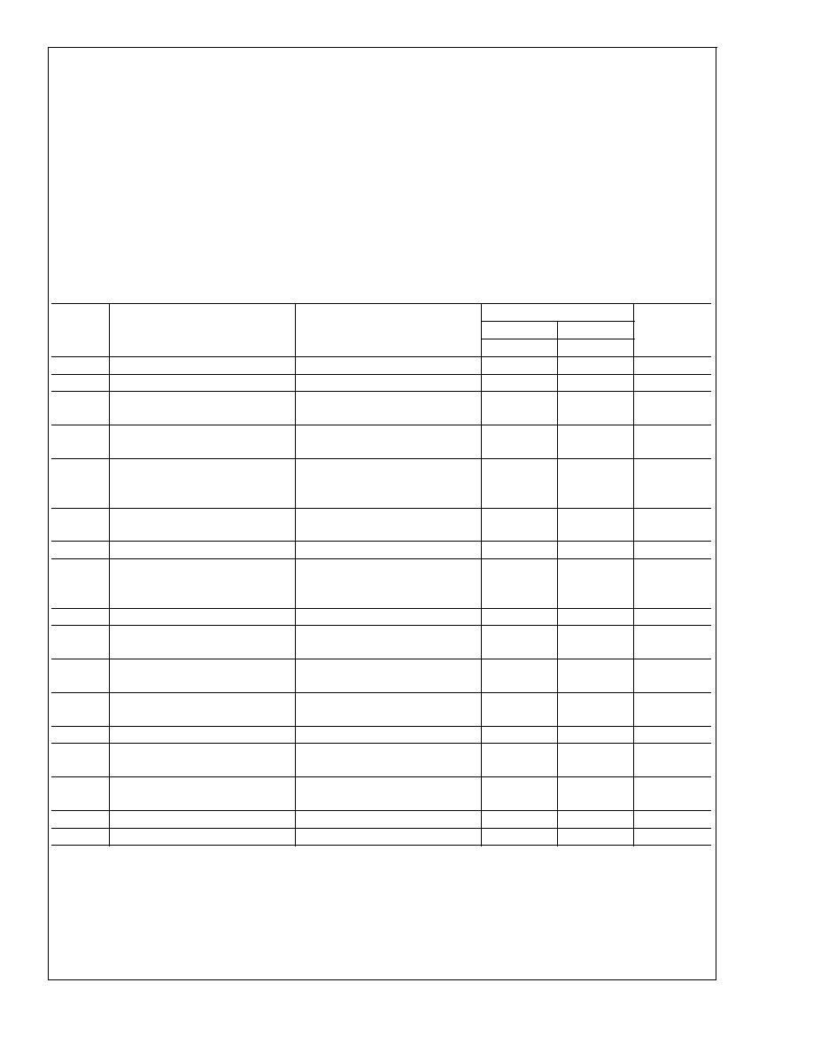
Electrical Characteristics DV
DD
= 3.0V, AV
DD
= 5.0V, R
L
= 32
(Notes 1, 2)
The following specifications apply for the circuit shown in Figure 1 unless otherwise specified. Limits apply for T
A
= 25�C.
Symbol
Parameter
Conditions
LM4921
Units
(Limits)
Typical
Limit
(Note 6)
(Notes 7, 9)
DV
DD
Digital Power Supply Voltage
Note 8
3.0
V
AV
DD
Analog Power Supply Voltage
Note 8
5.0
V
DI
DD
Digital Power Supply Quiescent
Current
R
Load
=
, f
MLCK
= 11.2896MHz
3.5
7.5
mA (max)
AI
DD
Analog Power Supply Quiescent
Current
R
Load
=
, f
MCLK
= 0MHz
6
10
mA (max)
I
SD
Total Shutdown Power Supply
Current
SHUTDOWN SPI bits 1 & 2 set to
logic 0,
SPI, M
CLK
and I
2
S inputs at GND
1
5
uA(max)
I
SB
Standby Current
Analog and Digital together
All clocks off
25
uA
V
FS
Full-Scale Output Voltage
Gain set at max
3.5
V
P-P
THD+N
Total Harmonic Distortion + Noise
f
IN
= 1kHz, P
OUT
= 12mW
(Vol Control = 11111, I
2
S input adj
to get 12mW at output)
0.03
%
P
O
Headphone Amplifier Output Power THD = (0.5%), f
OUT
= 1kHz
50
40
mW (min)
PSRR
Power Supply Rejection Ratio
AV
DD
C
BYPASS
= 2.0�F
V
RIPPLE
= 200mV
P-P
217Hz
62
45
dB (min)
SNR
Signal-to-Noise Ratio
f
IN
= 1kHz sinewave at -60dB
FS
,
A-weighted-f
CONV
= 44.1kHz
82
dB
DR
Dynamic Range
f
IN
= 1kHz sinewave at -60dB
FS
,
A-weighted
84
dB
A
CH-CH
Channel-to-Channel Gain Mismatch f
IN
= 1kHz
0.06
dB
X
TALK
Channel-to-Channel Crosstalk
f
CONV
= 44.1kHz,
f
IN
= 1kHz sinewave at -3dB
FS
72
dB
Volume Control Range
Minimum Attenuation
Maximum Attenuation
+3.0
-43.5
dB
dB
Volume Control Control Step Size
1.5
dB
Mute Attenuation
-102
dB
LM4921
www.national.com
5