 | –≠–ª–µ–∫—Ç—Ä–æ–Ω–Ω—ã–π –∫–æ–º–ø–æ–Ω–µ–Ω—Ç: LP3928 | –°–∫–∞—á–∞—Ç—å:  PDF PDF  ZIP ZIP |
LP3928
High Speed Bi-Directional Level Shifter and Ultra
Low-Dropout CMOS Voltage Regulator
General Description
The LP3928 is designed for portable and wireless applica-
tions with demanding performance and space requirements.
The LP3928 provides level shifting and power conversion
needed for applications interfacing differing voltage levels.
The part contains a bi-directional level shifter for three sig-
nals to translate the levels between 1.8V and 2.85V and an
ultra low-dropout CMOS 2.85V voltage regulator.
The three level shifted signals are individually direction con-
trolled. Signals going from 2.85V to 1.8V can also be latched
using an external clock source. The latches are powered
from internal 2.85V. There is also an option to by-pass the
latches.
The built-in low-dropout voltage regulator is ideal for mobile
phone and battery powered wireless applications. It provides
up to 150 mA from a 3.05V to 6.0V input, and is character-
ized by extremely low dropout voltage, low quiescent current
and low output noise voltage. It is stable with small 1.5 µF
±
30% ceramic and high quality tantalum output capacitors,
requiring smallest possible PC board area.
A shutdown mode is available for the level shifters and the
regulator. High performance is achieved over various load
conditions with very low rise and fall times.
Key Specifications
Level Shifter:
n
4 ns propagation delay (typ.)
n
2 ns rise and fall times (typ.)
n
20 ns direction switch response time
n
2 µA input/output leakage current
Low-Dropout Regulator:
n
3.05V to 6.0V input range
n
150 mA guaranteed output
n
Fast Turn-On time: 200 µs (typ.)
n
100 mV maximum dropout with 150 mA load
Features
n
Ultra small micro SMD package
n
Bi-directional level-shifter for three individual signals:
1.8V to 2.85V and 2.85V to 1.8V signal level translation
n
Logic controlled enable pins: 4 different operation
modes
n
LDO stable with ceramic and high quality tantalum
capacitors
n
Thermal shutdown
Applications
n
Multi-Media Cards for Cellular Phones
n
SD Cards for Cellular Handsets
n
Logic Level Translation
n
Portable Information Appliances
October 2002
LP3928
High
Speed
Bi-Directional
Level
Shifter
and
Ultra
Low-Dropout
CMOS
V
oltage
Regulator
© 2002 National Semiconductor Corporation
DS200391
www.national.com
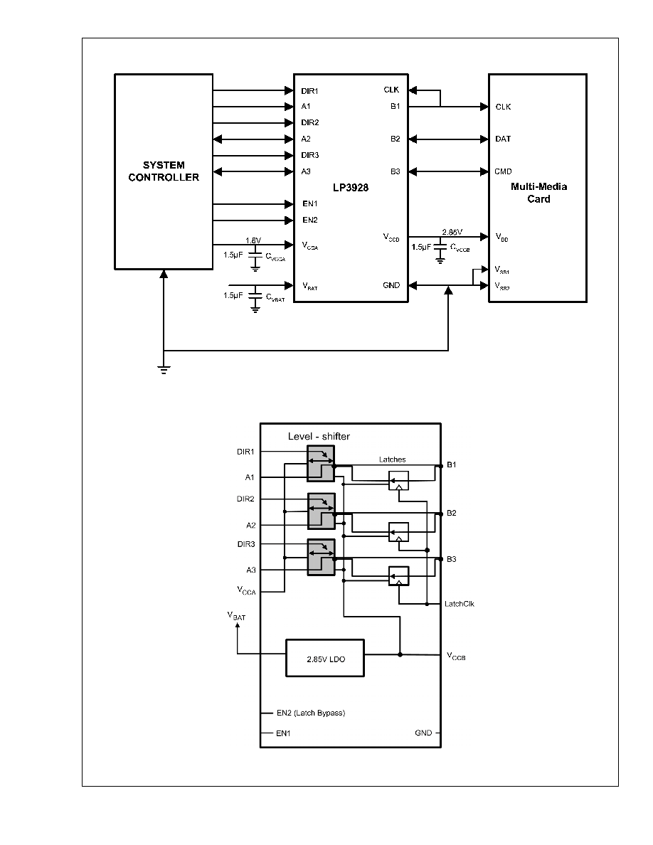
Typical Application Circuit
20039101
Block Diagram
20039102
LP3928
www.national.com
2
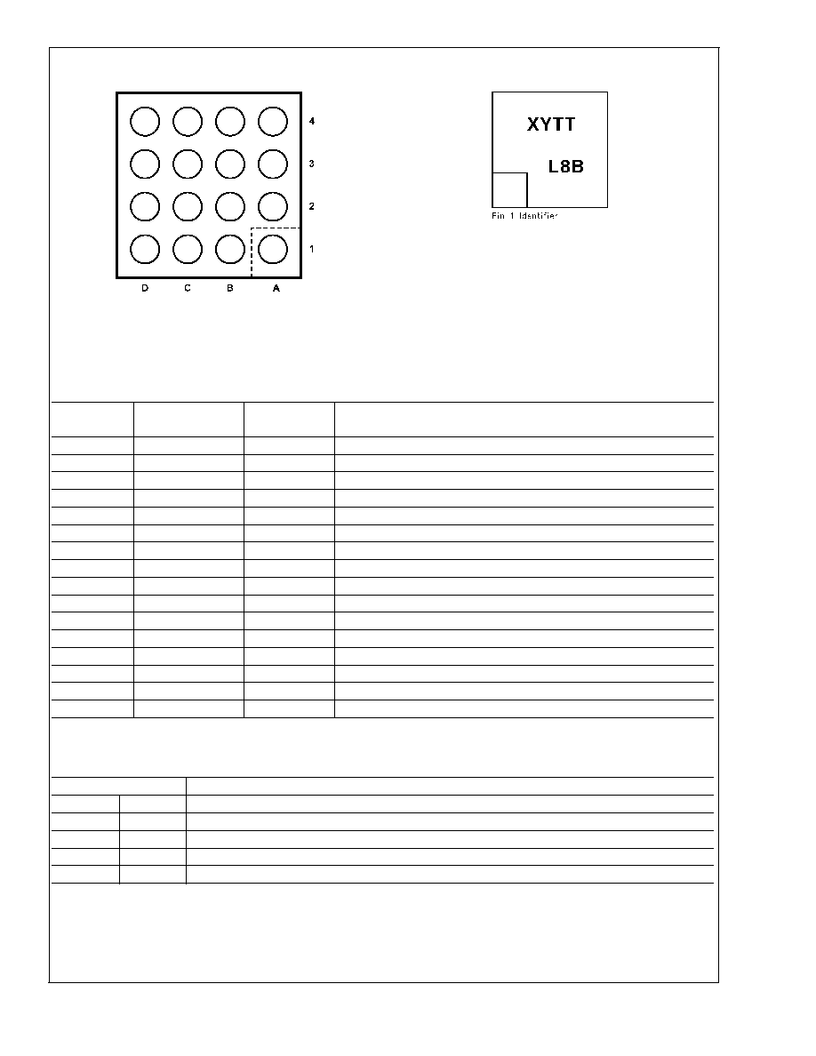
Package Outline and Connection Diagrams
20039103
Bottom View
16 Bump micro SMD Package
See NSC Package Number TLA16AAA
20039104
Note: The actual physical placement of the package marking will vary from
part to part. The package marking "XY" will designate the date code, "TT" is
a NSC internal code for die traceability. Both will vary considerably. L8B
identifies the device.
Top View
Pin Description
Pin Name
micro SMD
Bump Identifier
Logic Level
Function
A1
C4
1.8V
1.8V I/O Channel, (Note 1)
A2
D4
1.8V
1.8V I/O Channel, (Note 1)
A3
D3
1.8V
1.8V I/O Channel, (Note 1)
B1
C1
2.85V
2.85V I/O Channel, (Note 1)
B2
D1
2.85V
2.85V I/O Channel, (Note 1)
B3
D2
2.85V
2.85V I/O Channel, (Note 1)
DIR1
B3
1.8V
Direction control input Channel 1: `1': A
B; 0; BA
DIR2
B2
1.8V
Direction control input Channel 2: `1': A
B; 0; BA
DIR3
C3
1.8V
Direction control input Channel 3: `1': A
B; 0; BA
V
CCA
B4
IC supply to the 1.8V side
V
CCB
B1
IC supply, 2.85V output from LDO
V
BAT
A1
LDO supply, Battery voltage
GND
A3
Power ground connection
EN1
A4
1.8V
Mode pin 1, see Table 1 for modes and settings
EN2
A2
1.8V
Mode pin 2, see Table 1 for modes and settings
LatchClk
C2
2.85V
Clock input: rising edge latches B inputs (DIR=0, normal mode)
Note 1: Pin pairs A1≠B1, A2≠B2 and A3≠B3 form 3 independent bi-directional level-shifting channels.
TABLE 1. Operation Modes
Inputs
State
EN1
EN2
0
0
Level shifter off: High Z state on A
1
≠A
3
, B
1
≠B
3
, LDO off
0
1
Level shifter off: High Z state on A
1
≠A
3
, B
1
≠B
3
, LDO on
1
0
Latch bypassed in B to A direction, LDO=on (Note 2)
1
1
ON, normal mode (latch active)
Note 2: LatchClk is not used here. It should not be left floating.
LP3928
www.national.com
3
Pin Description
(Continued)
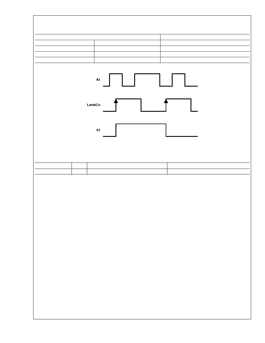
TABLE 2. Direction Control and LatchCLK (Normal Mode)
Inputs
Outputs and Direction
DIRx
LatchClk
1
X
Ax to Bx
0
No change (on Ax)
0
Bx to Ax, see example
Example for Latch Mode, DIR1 = `0', EN1 = EN2 = `1' (delay not shown):
20039105
Ordering Information
For micro SMD Package
Output Voltage (V)
Grade
LP3928 Supplied As 250 Units, Tape & Reel
LP3928 Supplied As 3000 Units, Tape & Reel
2.85
STD
LP3928TL-1828
LP3928TLX-1828
LP3928
www.national.com
4
Absolute Maximum Ratings
(Notes 3,
4)
If Military/Aerospace specified devices are required,
please contact the National Semiconductor Sales Office/
Distributors for availability and specifications.
V
BAT
, V
CCB
-0.2V to +6.5V
V
CCA
-0.2V to +3.3V
A
1
≠A
3
, EN, DIR
-0.2V to V
CCA
+ 0.2V
B
1
≠B
3
, LatchClk
-0.2V to V
CCB
+ 0.2V
Junction Temperature
150∞C
Storage Temperature
-65∞C to +150∞C
Lead Temperature (Note 27)
235∞C
Pad Temperature (Note 27)
235∞C
Power Dissipation (Note 5)
JA
(micro SMD), typical
180∞C/W
Maximum Power Dissipation
micro SMD
360 mW
ESD Rating (Note 6)
Human Body Model
2 kV
Operating Conditions
(Notes 3, 4)
V
BAT
3.05V to 6.0V
V
CCA
1.65V to 1.95V
V
CCB
(Note 7)
Junction Temperature
-40∞C to +125∞C
Ambient Temperature
-40∞C to +85∞C
Maximum Power Dissipation (Note 8)
220 mW
Electrical Characteristics
Unless otherwise specified: H = V
IH
min, L = V
IL
max, C
VBAT
= 1 µF, I
OUT
= 1
mA, C
VCCB
= 1 µF, C
VCCA
= 1 µF. Typical values and limits appearing in standard typeface apply for T
J
= 25∞C. Limits ap-
pearing in boldface type apply over the entire junction temperature range for operation, -40∞C to +125∞C. (Note 9)
Level Shifter DC Voltage Levels
Unless otherwise specified: EN1 = H, EN2 = X; 3.05V
V
BAT
6V, 1.65V V
CCA
1.95V.
Symbol
Parameter
Conditions
Min
Typ
Max
Units
V
IHA
High Level Input Voltage
For A Pins
V
CCA
*
0.65
V
CCA
+0.2
V
V
ILA
Low Level Input Voltage
0
V
CCA
*
0.35
V
V
OHA
High Level Output Voltage
For A Pins
I
OH
=4 mA
V
CCA
-0.45
1.5
V
CCA
+0.2
V
V
OLA
Low Level Output Voltage
I
OL
=4 mA
0
0.1
V
CCA
*
0.25
V
V
IHB
High Level Input Voltage
For B Pins
V
CCB
*
0.7
V
CCB
+0.2
V
V
ILB
Low Level Input Voltage
0
V
CCB
*
0.3
V
V
OHB
High Level Output Voltage
For B Pins
I
OH
=4 mA
V
CCB
*
0.7
2.75
V
CCB
+0.2
V
V
OLB
Low Level Output Voltage
I
OL
=4 mA
0
0.1
V
CCB
*
0.2
V
V
IHEN-DIR
High Level Input Voltage
For EN and DIR Pins
V
CCA
*
0.75
V
CCA
+0.2
V
V
ILEN-DIR
Low Level Input Voltage
0
V
CCA
*
0.27
V
V
IHLatClk
High Level Input Voltage
For LatchClk Pin
V
CCB
*
0.7
V
CCB
+0.2
V
V
ILLatClk
Low Level Input Voltage
0
V
CCA
*
0.3
V
Level Shifter DC Current Levels
Unless otherwise specified: EN1 = H, EN2 = X; V
BAT
= 6V or V
CCA
= 1.95V as applicable to B or A respectively.
Symbol
Parameter
Conditions
Min
Typ
Max
Units
I
IA
Input Leakage Current Ai
Vi
A
=0/1.9V, DIRi=H
(V
CCA
= 1.8V when Vi
A
= 1.9V)
0.001
±
2
µA
I
IDIR_EN
Input Leakage Current
DIR/EN
(Note 11)
Vi=0/1.9V (V
CCA
= 1.8V when Vi =
1.9V)
0.001
±
2
µA
I
IB
Input Leakage Current Bi,
LatchClk (Note 12)
Vi
B
=0/2.95V, DIRi=L
0.001
±
2
µA
I
CHA
B
Static I
CCB
Current/Channel
Static I
CCB
Current Total
(Notes 13, 17)
EN2=H, DIRi=H,
Total Includes I
BCOM
550
2050
875
3330
µA
I
CHB
A
Static I
CCB
Current/Channel
Static I
CCB
Current Total
(Notes 14, 17)
EN2=L, DIRi=L
Total Includes I
BCOM
2
406
30
840
µA
LP3928
www.national.com
5