LP3939
Power Amplifier Driver for Dual Band CDMA Handsets
General Description
Designed
specifically
for
Qualcomm's
MSM3xxx
and
MSM5xxx series, the LP3939 is an integrated device that
provides interface to the baseband processor to power-
switch two independent power amplifiers in dual band appli-
cations. By integrating the discrete components necessary
to achieve the same functions, the LP3939 drastically re-
duces board space and component cost.
Features
n
Power-switch for dual band CDMA power amplifier
Key Specifications
n
0.002 µA Quiescent Current (typ)
n
LLP16 Package
Applications
n
Dual-band CDMA phones with MSM3xxx or MSM5xxx
platform
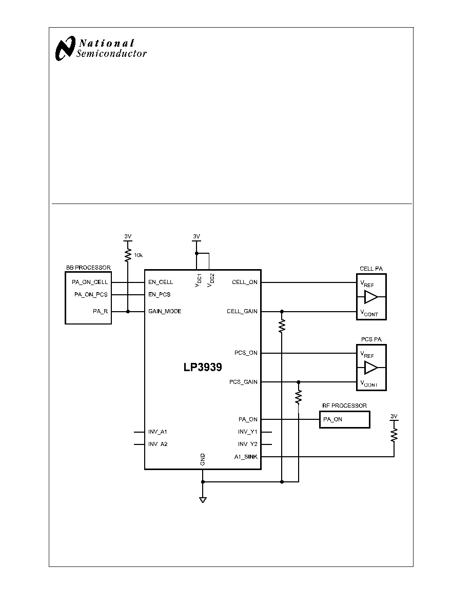
LP3939 Application Circuit
20083101
Note: This application circuit shows the connection interface to a typical Skyworks PA. Connections to other PA vendors may vary slightly.
November 2003
LP3939
Power
Amplifier
Driver
for
Dual
Band
CDMA
Handsets
© 2003 National Semiconductor Corporation
DS200831
www.national.com
Connection Diagram
(LLP16: NSC Marketing Drawing LQA16A)
20083102
Top View
See NS Package Number LQA16A
Pin Description
Pin
Name
Functional Description
1
INV_A1
Input
2
V
DD2
Supply. V
DD1
and V
DD2
must be
tied together externally.
3
PCS_ON
Output, open drain
4
PCS_GAIN
Output, open drain
5
INV_Y1
Output
6
GAIN_MODE
Input
7
EN_CELL
Input
8
EN_PCS
Input
9
CELL_GAIN
Output, open drain
10
CELL_ON
Output, open drain
11
V
DD1
Supply. V
DD1
and V
DD2
must be
tied together externally.
12
PA_ON
Output
13
INV_A2
Input
14
INV_Y2
Output, open drain
15
GND
GND
16
A1_SINK
Output, open drain
Ordering Information
LP3939 Supplied as 1k Units, Tape and Reel
LP3939 Supplied as 4.5k Units, Tape and Reel
Package Marking
LP3939ILQ
LP3939ILQX
National Logo
UZXYTT
LP3939
Note:
U-wafer fab code
Z-assembly plant code
XY-date code
TT-die run traceability
LP3939
www.national.com
2
Absolute Maximum Ratings
(Notes 1,
2)
If Military/Aerospace specified devices are required,
please contact the National Semiconductor Sales Office/
Distributors for availability and specifications.
V
DD1
, V
DD2
-0.3V to +6.0V
EN_CELL, EN_PCS,
GAIN_MODE, INV_A1,
INV_A2, PA_ON, INV_Y1,
CELL_ON, CELL_GAIN,
PCS_ON, PCS_GAIN, INV_Y2
and A1_SINK
-0.3V to (V
DD
+ 0.3V)
GND to GND SLUG
±
0.3V
Junction Temperature
150∞C
Maximum Power Dissipation
(Note 3)
2.0W
Storage Temperature
-65∞C to +150∞C
ESD (Note 4):
Human Body Model
2 kV
Machine Model
200V
Operating Ratings
(Notes 1, 2)
V
DD1
, V
DD2
1.8V to 5.5V
Junction Temperature
-40∞C to +125∞C
Operating Temperature
-40∞C to +85∞C
Thermal Resistance
JA
(LLP16)
39.8∞C/W
Maximum Power Dissipation
(Note 5)
1.38W
DC Electrical Characteristics
Unless otherwise noted, V
DD1
= V
DD2
= 3V. Typical values and limits appearing in normal type apply for T
J
= 25∞C. Limits ap-
pearing in boldface type apply over the entire junction temperature range for operation, -40∞C to +85∞C. (Note 6)
Symbol
Parameter
Conditions
Typ
Limit
Units
Min
Max
I
IN
Input Current
All Input Pins
0.05
5
µA
I
Q
Quiescent Current
All inputs tied to V
DD
or ground.
No load at the outputs.
0.002
5
µA
I
LEAKAGE
Output Leakage Current
CELL_ON, PCS_ON
CELL_GAIN, PCS_GAIN
10
µA
A1_SINK
5
R
DS-ON
MOSFET's ON Resistance
P-Ch, V
DD
= 3V
CELL_ON, PCS_ON
CELL_GAIN, PCS_GAIN
275
500
m
P-Ch, V
DD
= 2V
CELL_ON, PCS_ON
CELL_GAIN, PCS_GAIN
430
650
V
IH
Logic High Input
1.8V
V
DD
<
2.5V
EN_CELL, EN_PCS, INV_A1,
GAIN_MODE, INV_A2
1.4
V
2.5V
V
DD
3.5V
EN_CELL, EN_PCS, INV_A1,
GAIN_MODE, INV_A2
2.0
V
IL
Logic Low Input
1.8V
V
DD
3.5V
EN_CELL, EN_PCS, INV_A1,
GAIN_MODE, INV_A2
0.4
V
V
OH
Logic High Output
PA_ON, INV_Y1,
I
SOURCE
= 1 mA
2.93
2.8
V
INV_Y2,
I
SOURCE
= 1 mA
2.74
2.5
V
OL
Logic Low Output
PA_ON, INV_Y1, I
SINK
= 1 mA
80
200
mV
INV_Y2, A1_SINK
I
SINK
= 1 mA
16
55
LP3939
www.national.com
3
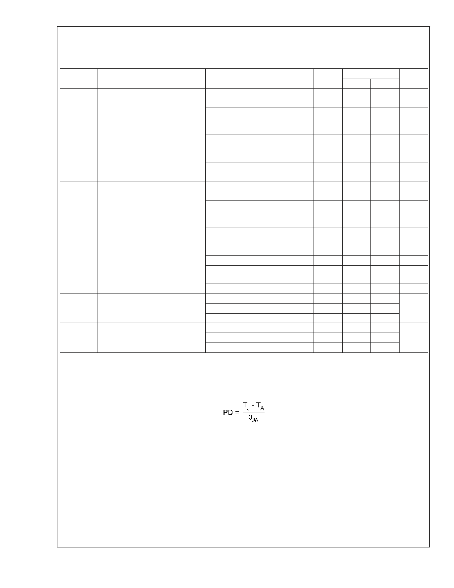
AC Electrical Characteristics
Unless otherwise noted, V
DD1
= V
DD2
= 3V, C
LOAD
= 50 pF. Typical values and limits appearing in normal type apply for T
J
=
25∞C. Limits appearing in boldface type apply over the entire junction temperature range for operation, -40∞C to +85∞C.
(Note 7)
Symbol
Parameter
Conditions
Typ
Limit
Units
Min
Max
t
PLH
Propagations Delay
Low to High
EN_CELL to PA_ON or
EN_PCS to PA_ON
10
80
ns
EN_CELL to CELL_ON or
EN_PCS to PCS_ON
R
PD
= 100
7
56
ns
GAIN_MODE to CELL_GAIN
or GAIN_MODE to PCS_GAIN
R
PD
= 100
7
56
ns
INV_A1 to INV_Y1
10
80
ns
INV_A2 to INV_Y2
25
200
ns
t
PHL
Propagations Delay
High to Low
EN_CELL to PA_ON or
EN_PCS to PA_ON
10
80
ns
EN_CELL to CELL_ON or
EN_PCS to PCS_ON
R
PD
= 100
25
200
ns
GAIN_MODE to CELL_GAIN
or GAIN_MODE to PCS_GAIN
R
PD
= 100
20
160
ns
INV_A1 to INV_Y1
10
80
ns
INV_A1 to A1_SINK
R
PU
= 10 k
5
40
ns
INV_A2 to INV_Y2
5
40
ns
t
RISE
Rise Time
PA_ON
15
120
ns
INV_Y2
50
400
INV_Y1
20
160
T
FALL
Fall Time
PA_ON
15
120
ns
INV_Y2
10
80
INV_Y1
20
160
Note 1: Absolute Maximum Ratings are limits beyond which damage to the device may occur. Operating Ratings are conditions under which operation of the device
is guaranteed. Operating Ratings do not imply guaranteed performance limits. For guaranteed performance limits and associated test conditions, see the Electrical
Characteristics tables.
Note 2: All voltages are with respect to the potential at the GND pin.
Note 3: The Absolute Maximum power dissipation depends on the ambient temperature and can be calculated using the formula:
where T
J
is the junction temperature, T
A
is the ambient temperature, and
JA
is the junction-to-ambient temperature. The 2.0W rating appearing under Absolute
Maximum Ratings results from substituting the Absolute Maximum junction temperature, 150∞C for T
J
, 70∞C for T
A
and 39.8∞C/W for
JA
. More power can be
dissipated safely at ambient temperatures below 70∞C. Less power can be dissipated safely at ambient temperatures above 70∞C. The Absolute Maximum power
dissipation can be increased by 25 mW for each degree below 70∞C, and it must be derated by 25 mW for each degree above 70∞C.
Note 4: The human body model is 100 pF discharged through a 1.5 k
resistor into each pin. The machine model is a 200 pF capacitor discharged directly into
each pin.
Note 5: Like the Absolute Maximum power dissipation, the maximum power dissipation depends on the ambient temperature. The 1.38W rating appearing under
Absolute Maximum Ratings results from substituting the Maximum junction temperature, 125∞C for T
J
, 70∞C for T
A
and 39.8∞C/W for
JA
. More power can be
dissipated safely at ambient temperatures below 70∞C. Less power can be dissipated safely at ambient temperatures above 70∞C. The Absolute Maximum power
dissipation can be increased by 25 mW for each degree below 70∞C, and it must be derated by 25 mW for each degree above 70∞C.
Note 6: All limits are guaranteed by testing or statistical analysis.
Note 7: All AC parameters are guaranteed by design, not production tested.
LP3939
www.national.com
4