 | –≠–ª–µ–∫—Ç—Ä–æ–Ω–Ω—ã–π –∫–æ–º–ø–æ–Ω–µ–Ω—Ç: RA1133J | –°–∫–∞—á–∞—Ç—å:  PDF PDF  ZIP ZIP |
www.perkinelmer.com/opto
RA1133J Full Frame CCD Image Sensor
24 µm square pitch, 1100 x 330 pixel configuration
D
A
T
ASHEET
Imaging
Imaging Product Line
∑
Two stage TE cooler integrated into
the package
∑
Hermetically sealed
∑
10 MHz data rate
∑
100% fill factor
Description
Features
∑
363,000 picture elements (pixels) in
a 1100 x 330 configuration
∑
24 µm square pixels
∑
2-phase buried channel process
∑
On-chip amplifier for low noise and
high speed readout
∑
Dynamic range greater than 25,000:1
∑
On-chip temperature sensor
Caution: While the RA1133J imagers have
been
designed to resist electrostatic discharge (ESD),
they can be damaged from such discharges.
Always observe proper ESD precautions when
handling and storing these sensors.
DSP-303.01C- 8/2002W Page 1
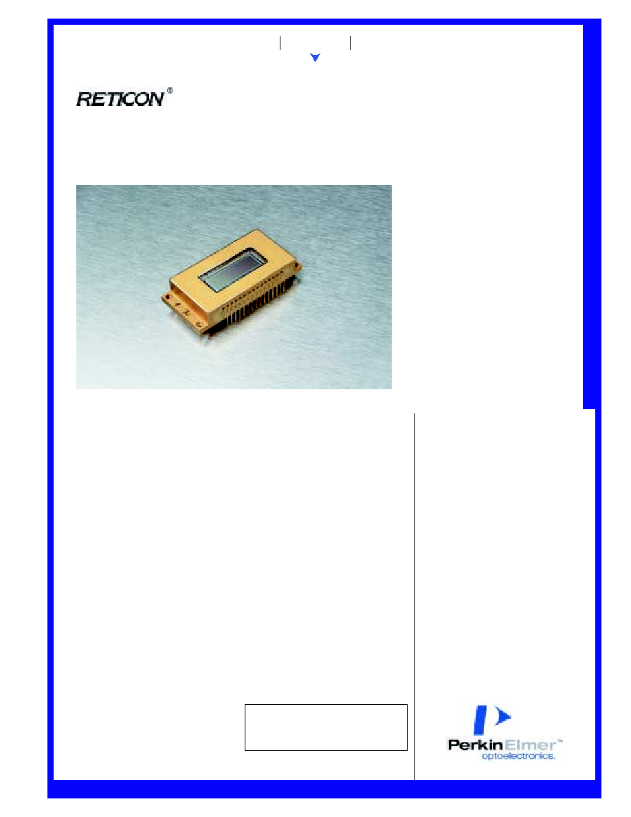
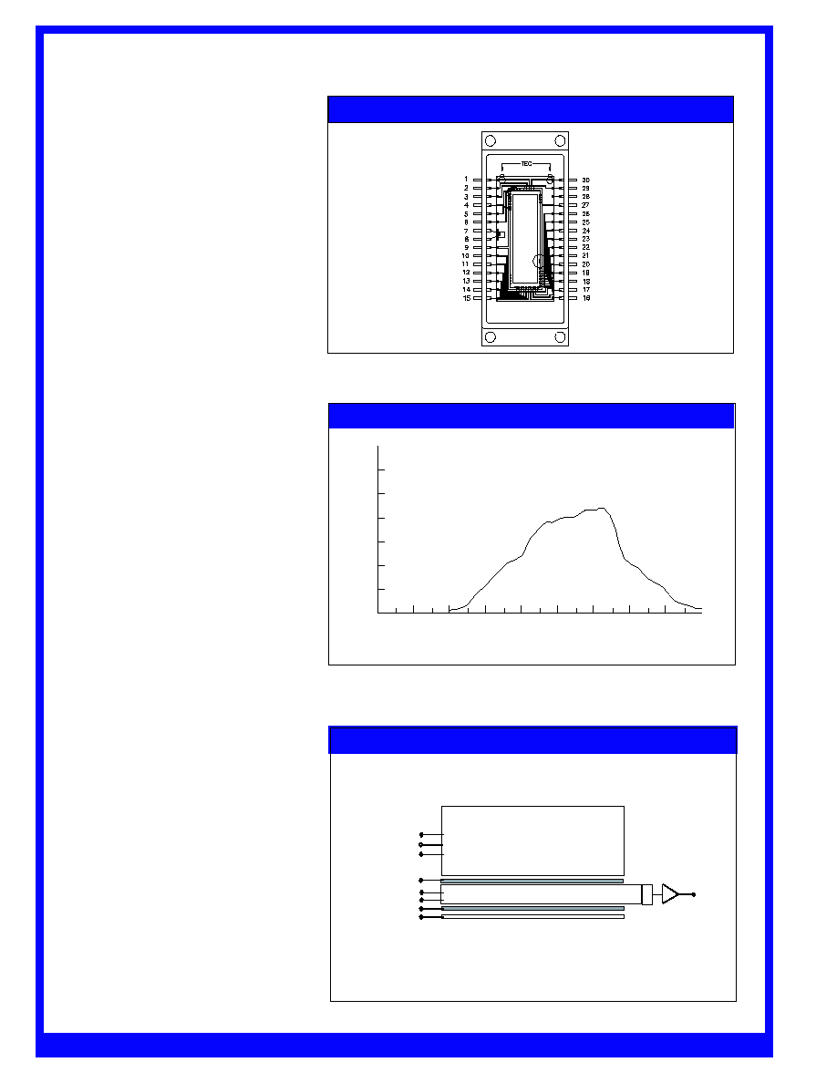
The RA1133J is a full frame CCD
sensor with reset capabilities designed
specifically for use in spectroscopy,
biomedical imaging and related scientific
imaging applications. The package for
the array is designed with an integrated
two stage thermoelectric cooler. This
enables the device to be run 40∞ C
below ambient temperature, -15∞ C
when compared to room temperature.
Its combination of very low noise and
low dark current make it ideal for low
light, high dynamic range and high
resolution applications.
The imager is structured with a single
output register at one end of the imaging
columns. A lateral reset drain is located
adjacent to this readout register which
enables the dumping of accumulated
charge from the array. Two phase clocks
are needed to drive the readout register.
Three phase clocks are needed to drive
imaging cells. The array is available in
a 30-pin metal package with an integrated
TE cooler as shown in Figure 1. Package
dimensions are shown in Figure 8.
MPP Operation
A major source of dark current in
devices such as this originates in
surface states at the Si-SiO2 interface.
A unigue design and process enables
the RA1133J to be run in "multi-pinned
phase" or MPP mode of operation.
This helps eliminate dark current
generation in the interface surface
states. By holding the vertical clocks
at negative potential during integration
and horizontal signal readout, the
surface will not be depleted and the
surface state will not generate dark
current.
Full Frame CCD Sensor
www.perkinelmer.com/opto
DSP-303.01C - 8/2002W Page 2
Imaging Area
The imaging area is an array of 1100
columns (vertical CCD shift registers).
Each column has 330 picture elements.
The pixel size is 24 µm by 24 µm. The
total imaging area is 26.4 mm by 7.92 mm.
Typical spectral response as a function
of wavelength is shown in Figure 2.
This is for both the standard array and
an array coated with lumogen, an UV
phosphor that extends the range of the
detector into the ultraviolet.
In the vertical direction, each pixel
corresponds to one stage (three electrodes)
of the shift register. The three electrode
groups are driven by three-phases (ÿ1V -
ÿ3V) brought in from both edges of the
array to improve clock electrode response
time. Charge packets (imaging data) in the
vertical register can be shifted to the hori-
zontal readout by clocking the three phases
(ÿ1V, ÿ2V and ÿ3V). A transfer gate (ÿTG) is
provided at the interface of the vertical reg-
ister. The transfer gate controls the transferring
of charge into the horizontal readout register.
Charge flow is from ÿ3 gate of the vertical
shift register into ÿ1 gate of the horizontal
readout register. The control function is
performed by pulsing the transfer gate high
to permit the charge flow from the vertical
register into the horizontal register for
readout. When the potential of the vertical
register electrodes is held steady, a potential
well is created beneath the storage gates
ÿ1V and ÿ2V. When an image impinges
on the sensing area, an electrical signal of
the scene will be collected in the potential
well during this integration period.
Following the integration interval, the
collected charge (signal) in the array can
be read out as a full frame image by
transferring the charge, one or more rows at
a time, into the horizontal shift register.
From here, the charge can be shifted serially
to the output amplifier. A mechanical
shutter is needed to shield the array from
incident light during the readout process.
A strobe illumination could be used to
stimulate the shuttered mode of operation.
Image smearing degrades the performance,
particularly at low data rates, unless
shuttering is provided.
Figure 1. Pinout Configuration
ÿ1V
+
-
ÿ3V
ÿTG2
VLD
ÿLG2
LS
TEMP+
TEMP-
VSUB
ÿTG2
ÿ3V
ÿ1V
ÿ2V
ÿTG1
ÿSG
ÿ2V
ÿTG1
N/C
VSUB
LS
ÿ1H
ÿ2H
ÿLG1
VDD
VOUT
V LD
VSS
VRD
ÿRG
VOG
500
600
700
800
900
1000
1100
Wavelength, nm
10
0
20
30
40
50
60
Quantum Efficienc
y (%)
400
300
200
Figure 2. Quantum Efficiency
Horizontal CCD Shift
Imaging Area
1100 (H) x 330 (V) - active pixels
ÿTG
Output Buffer
Figure 3. Functional Diagram
ÿ1V
ÿ2V
ÿ3V
ÿ1H
ÿ2H
ÿLG
VLD
The horizontal shift register is driven by
two phase clocks (ÿ1H and ÿ2H). The
horizontal register has 1100 stages plus
an extension of 35 stages ( 3 dummy stages,
16 leading isolation stages and 16 trailing
isolation stages). As a result, amplifier
power is dissipated more efficiently and
dark current generation by localized heating
is minimized.
Horizontal Register
Full Frame CCD Sensor
www.perkinelmer.com/opto
DSP-303.01C - 8/2002W Page 3
Summing Mode
At the end of the horizontal register, there is
an ouput summing well which can be clocked
to allow multiple-pixel summation of the
scene. This summing well is located after
the 19 extra stages of the horizontal register
and prior to the DC biased gate (VOG) as
shown in Figure 5. The summing gate (ÿSG)
can be clocked with one of the horizontal
clock phases or with its own clock generator
(see Figure 4a for summing gate timing). For
example, two parallel lines of charge are
additively transferred into the serial register,
then the summing gate is pulsed low after
the charge from two serial pixels has been
transferred into the summing well. Thus,
the resulting signal represents the sum of
charges in four (2x2) contiguous pixels from
the imaging region. It effectively reduces
the 1100 x 330 device to a 550 x 165 array
and increases the pixel size by four times.
Other variations of this technique can be
useful for low-light level situations, i.e.,
scenes with low contrast or a low signal-to-
noise ratio. There is, of course, a loss in
resolution that accompanies the gain in
effective pixel size.
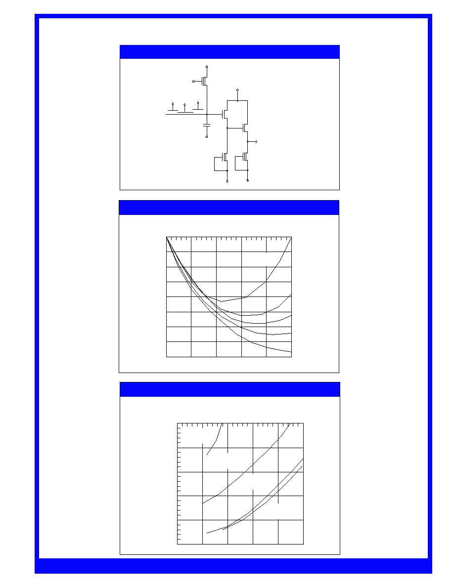
Output Amplifier
There is an on-chip amplifier that is
located at the end of the extended shift
register. The amplifier is a two stage
buried channel transistor amplifier as
shown in Figure 5. It is designed to operate
with data rates in excess of 10 MHz. It
has a bandwidth of approximately 60 MHz
with a 10 pF load.
Temperature Monitoring
The RA1133J device has a temperature
sensor integrated into the package for
monitoring array temperature.
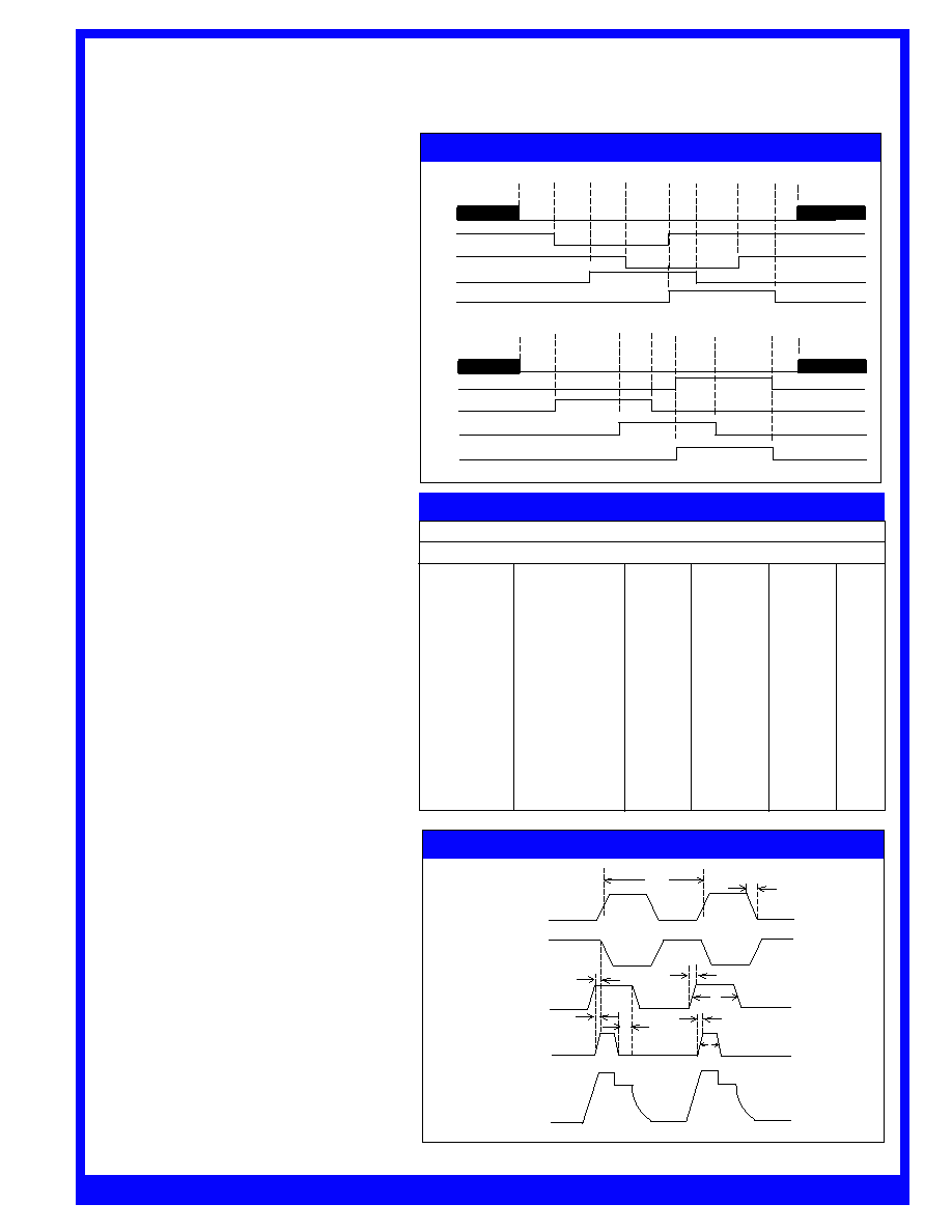
Timing Requirements
The timing recommended to run the RA1133J
imager in the low speed and low noise mode of
operation is shown in Figures 4A, 4B, and 4C. A
50% duty cycyle, two phase clock will drive the
horizontal register to its highest speed. Figure 4a
shows the timing of the horizontal two phase
clocks, summing well clock and reset clock. To
achieve high charge transfer, serial clocks must
cross between 10% and 90% of the peak voltage.
In addition, the rise and fall times of the two
phase clocks need to be more than 50 ns in order
to prevent the injection of spurious charge into
the CCD channel.
Table
Table 2. Vertical Timing Diagram Characteristics
Item
Sym
Min
Typ
Max
Units
FE H1 to FE 1V
t1
µs
2.6
FE 1V to RE 3V
t2
µs
2.6
RE 3V to FE 2V
t3
µs
2.6
FE 2V to RE 1V
t4
µs
5.2
Figure 4C. Horizontal CCD Shift Register Timing
H1
1V
2V
3V
TG
Normal Mode
t1
t1
t2
t2
t3
t3
t4
t4
t5
t5
t6
t6
t7
t7
t8
t8
H1
1V
2V
3V
TG
MPP Mode
t9
t9
t10
t10
t11
t11
t12
t12
t13
t13
t14
t14
t15
t15
RE 1V to FE 3V
t5
µs
1.4
FE 3V to RE 2V
t6
µs
1.4
RE 2V to FE TG
t7
µs
4.6
FE TG to RE H1
t8
µs
2.6
FE H1 to RE 2V
t9
µs
2.6
RE 2V to RE 3V
t10
µs
5.2
RE 3V to FE 2V
t11
µs
2.6
FE 2V to RE 1V
t12
µs
2.6
RE 1V to FE 3V
t13
µs
2.8
FE 3V to FE TG
t14
µs
4.6
FE TG to RE H1
t14
µs
2.6
Figure 4a. Horizontal CCD Shift Register Timing
Video
Output
ÿRS
ÿSG
ÿ2H
ÿ1H
t3
t3
t1
t1
t2
t2
t4
t4
t9
t9
t7
t7
t6
t6
t5
t5
t8
t8
www.perkinelmer.com/opto
Full Frame CCD Sensor
Timing Requirements
(cont.)
DSP-303.01C - 8/2002 Page 4
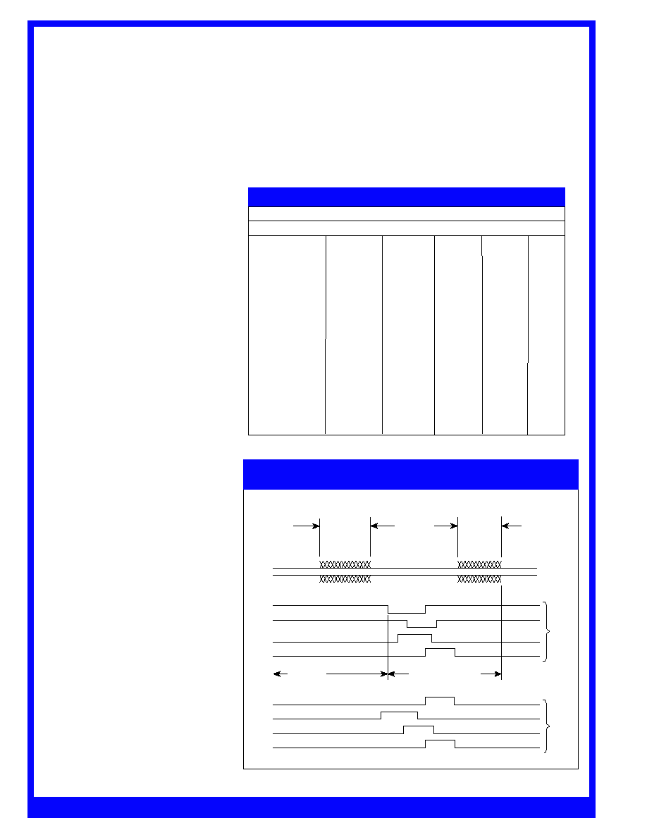
The timing shown in Figure 4a is
repeated 1100 + 35 (or more) times
to allow the readout of one complete
line of the image.
Figure 4b shows the timing require-
ments for the vertical register. Over-
lapping of the vertical clocks are
normally longer than 5 µs. Rise and
fall times of all clocks need to be 3 µs
or longer in order to prevent spurious
charge into the CCD channel. All
vertical clock transitions should occur
when the horizontal clocks are held
steady.
Timing for MPP and normal mode is
shown. The difference between the
two modes is that during integration,
all clocks must be held low for MPP
mode.
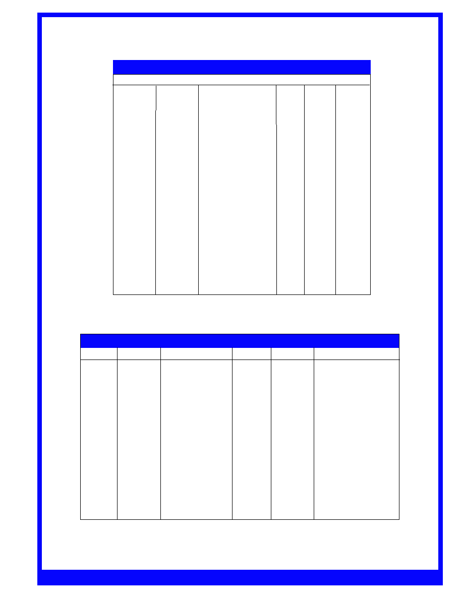
Array Cooling
Both the dark current and the noise
performance of the array can be im-
proved by cooling. The dark current
will be reduced by 50% for approx-
imately every 6 - 8 ∞ C reduction in
array temperature. Cooling can be
achieved via the integrated thermo-
electric cooler. The bias supplies TEC+
and TEC- electronically control this
cooler. This is a two-stage cooler
capable of reducing the temperature
of the array 40∞ C from the ambient
temperature. Additional cooling can be
achieved by decreasing the ambient
temperature or by cooling the heat sink
on the TE cooler as shown in Figure 6
and Figure 7.
Region of Interest
Rapid access to regions of interest is
facilitated by use of a lateral charge
drain. The drain is constructed adjacent
to the horizontal CCD (HCCD) shift register.
Unwanted lines of data are quickly dis-
posed without the requirement for hori-
zontal transfer. In this manner, entire lines
of image data can be disposed of by a single
vertical shift sequence, with a time penalty
of 20 µs. This is to be contrasted with the
normal read sequence which includes both
the vertical shift (20 µs), plus readout of
the 1130 horizontal elements (2260 µs).
As the unwanted lines are transferred from
storage region into the HCCD, the hori-
zontal phases are held high to maintain a
surface
potential which is more positive than the low state
channel potential of the transfer gate. Similar to a
lateral antiblooming drain, charge will spill prefer-
entially into the rapid discharge drain. Due to the
fixed potential barrier, the HCCD cannot be
completely cleared of charge and thus one horizontal
shift sequence is required before resumption of valid
data read.
Figure 4b. Vertical CCD Shift Register Timing and Its Relationship to
Horizontal Clocks in Normal and MPP Mode
¯TG
¯3V
¯2V
¯1V
¯2H
¯1H
¯TG
¯3V
¯2V
¯1V
1135 (+) ¯
Clock Cycles
to read 1 line
Normal
Mode
MPP
Mode
End
Integration
Period
Quiescent
State of All
Horizontal
Phases
During ¯
C
Transitions
Repeat 330(+) Times to
Read Out the Entire Image
Horizontal
Clear Out 1
1135 (+) ¯
Clock Cycles
Start
Integration
Period
Table 1. Timing Diagram Characteristics
Item
Sym
Min
Typ
Max
Units
¯
rise/fall time
T1
1, 2H
T2
+0
100
100
ns
50
ns
ns
ns
ns
50
ns
10
ns
ns
+0
50
ns
+0
T3
T4
¯
1, 2H
¯
SG
¯
SG
¯
RG
¯
SG
¯
RG
¯
RG
¯
SG
clock period
delay from
¯
H2
edge
rise/fall time
delay from
¯
SG
edge
delay from
¯
RG
edge
rise/fall time
pulse duration
pulse duration
T5
T6
T7
T8
T9
Full Frame CCD Sensor
www.perkinelmer.com/opto
DSP-303.01C - 8/2002 Page 5
Figure 7. Heat Sink Temperature vs. Chip Temperature
-50
-40
-30
-20
-10
0
20
30
40
50
60
10
Heat Sink Temperature
T
Hot
, C
Chip T
e
mper
ature
T
CPLP
, C
I = .5A
TEC Current
I = 1.1A
TEC Current
I = 2.0A
TEC Current
I = 2.5A
TEC Current
Figure 6. TEC Current vs. Chip Temperature (Ambient Temperature)
-80
-70
-60
-50
-40
-30
-20
-10
0
.5
1.0
1.5
2.0
2.5
0
Current to Thermo-Electric Cooler, Amp
T
Chip
≠
T
Ambient
, C
2.3
∞ C/W
Heat Sink
1.8C/W
Heat Sink
1.3
C/W
Heat Sink
.5
C/W
Heat Sink
0
C/W
Heat Sink
VSS
VSS
VOUT
VSUB
Two Stage Amplifier
VDD
VRD
ÿRG
ÿ1H
ÿSG
VOG
Figure 5. Output Structure

www.perkinelmer.com/opto
Full Frame CCD Sensor
DSP-303.01C - 8/2002W Page 6
Figure 8. Package Dimensions
2.320
(58.93)
2.530
(64.26)
1.150
(29.21)
30
16
1
15
0.105
(2.667)
1.100
(27.94)
0.880
(22.35)
0.440
(11.18)
0.158
(4.013)
0.110
(2.794)
0.523
(13.28)
Pixel 1
4 x
ÿ
0.125 holes
1.400
(35.56)
0.100
(2.540)
0.565
(14.35)
30 x
ÿ
0.025 pin
0.451
+
/
-
0.010
Image Center
Die Apeture
(11.45
+
/
-
0.254)
Bottom surface to image surface
0.115
+
/
-
0.010
(2.921
+
/
-
0.254)
Image surface to inside of window
TEC -
TEC +
0.600
(15.24)
1.300
+
/
-
0.015
(33.02
+
/
-
0.381)
0.420
(10.67)
0.330
(8.382)
0.620
(15.74)
2 x
ÿ
0.08 pin
(Both sides)
Measurements in inches (millimeters)
Table 3. Absolute Maximum Ratings
Min Max
Storage Temperature
+ 85C
+ 85C
- 55C
- 55C
Operating Temperature
Table
Table 4. Typical Device Specifications
Parameter
Sym Min
Typ
Max
Units
15
Format
26.4 x 7.92
25,000:1
24 x 24
1000
0.9999
4
1200
1
3
300
250
µm
mm
Ke-
mV
pA/cm2
±%
0.99995
±%
µV/e-
MHz
1100 x 330
e-
DR
Pixel Size
Imaging Area
Dynamic Range
Full Well Charge
Saturation Voltage
Dark Current MPP
Photo Response
Non Uniformity
Dark Signal Uniformity
Charge Transfer Efficiency
Output Amplifier Gain
Operating Frequency
Read Noise
10
Q
V
DL
PRNU
DSNU
CTE
fclock
1
SAT
3
2
10
5
2
5
SAT
4
Notes:
1. Full well/read noise, MPP mode
2. RLoad = 5.1 kOhms, MPP mode
3. MPP mode at -15 ∞C
4. Measured at 500 kHz a t -15 ∞C
www.perkinelmer.com/opto
Full Frame CCD Sensor
DSP-303.01C - 8/2002W Page 7
Table 3.
Table 5. Recommended Operating Conditions
Pin #
Signal
Function
Typ
Tolerance
24, 25
ÿ1H, ÿ2H
Horizontal Clocks
ÿTG
ÿSG
ÿ1V (MPP)
3, 29
15
1, 12
2, 11, 13, 30
5, 23
17
16
22
4, 20
18
6, 26
19
9, 27
ÿ2V, ÿ3V
ÿLG
ÿRG
VOG
VDD
VLD
VRD
LS
VSS
VSUB
Reset Gate
Lateral Charge Gate
Vertical Clocks
Vertical Clock (MPP Phase)
Summing Gate Clock
High
4
Low
-8
High
5
Low
0
Low
-9
High
Low
-11
High
5
Low
0
High
8
Low
0
High
4
Transfer Gate Clock
Low
0
Substrate Bias
Video Amplifier Source
Light Shield
Amplifier Reset Drain
Lateral Charge Drain
Amplifier Voltage Supply
Output Gate
High
5
2
GND
GND
10
13
14
3
-2
±10%
±5%
±5%
±10%
±5%
±5%
±5%
±5%
±5%
±5%
±5%
±5%
±5%
±5%
Table 6. Pinout Descriptions
Pin #
Sym
Function
Pin #
Sym
Function
ÿ
1V
ÿ
3V
ÿ
TG2
V
LD
ÿ
LG2
V
SUB
ÿ
TG2
Vertical Phase 1
Vertical Phase 3
Lateral Charge Drain
Lateral Charge Gate 2
Light Shield
Temp+
Temp-
Substrate
Vertical Phase 3
Vertical Phase 1
Vertical Phase 2
Transfer Gate 1
Summing Gate
Transfer Gate 2
Transfer Gate 2
LS
TEMP+
TEMP-
ÿ
3V
ÿ
2V
ÿ
1V
ÿ
TG1
ÿ
SG
ÿ
RG
V
RD
V
SS
V
LD
V
OUT
V
DD
ÿ
LG1
ÿ
2H
ÿ
1H
LS
V
SUB
N/C
ÿ
TG1
ÿ
2V
V
OG
Output Gate
Reset Gate
Reset Drain
Video Amplifier Source
Lateral Charge Drain
Video Output
Lateral Charge Gate 1
Horizontal Phase 2
Horizontal Phase 1
Light Shield
Substrate
No Connection
Transfer Gate 1
Vertical Phase 2
Video Amplifier Drain
1
2
4
5
6
7
8
9
11
12
13
14
15
10
3
16
17
19
20
21
22
23
24
26
27
28
29
30
25
18
www.perkinelmer.com/opto
For more information e-mail us at
© 2001 PerkinElmer Inc. All rights reserved.
PerkinElmer, the PerkinElmer logo and the stylized "P" are trademarks of PerkinElmer, Inc.
DSP-303.01C - 8/2002W
Reticon is a registered trademark of PerkinElmer, Inc.
Full Frame CCD Sensor
Page 8
Table 8. Sales Offices
North America
United States
PerkinElmer Optoelectronics
2175 Mission College Blvd.
Santa Clara, CA 95054
Toll Free: 800-775-OPTO (6786)
Phone: +1-408-565-0830
Fax: +1-408-565-0703
Europe
Germany
PerkinElmer Optoelectronics GmbH
Wenzel-Jaksch-Str. 31
D-65199 Wiesbaden, Germany
Phone: +49-611-492-570
Fax: +49-611-492-165
Asia
Japan
PerkinElmer Optoelectronics
NEopt. 18F, Parale Mitsui Building 8
Higashida-Cho, Kawasaki-Ku
Kawasaki-Shi, Kanagawa-Ken 210-0005 Japan
Phone: +81-44-200-9170
Fax: +81-44-200-9160
www.neopt.co.jp
Singapore
47 Ayer Rajah Crescent #06-12
Singapore 139947
Phone: +65-770-4925
Fax: +65-777-1008
Ordering Information
While the information provided in
this data sheet is intended to describe
the form, fit and function for this
product, PerkinElmer reserves the
right to make changes without notice.
Part Number
RA1133JAS-912
Table 7. Ordering Information
For more information e-mail us at
opto@perkinelmer.com or visit our web
site at www.perkinelmer.com/opto.
All values are nominal; specifications
subject to change without notice.