
TONE DECODER S1T0567
1
INTRODUCTION
The S1T0567 is a monolithic phase-locked loop system designed to
provide a saturated transistor switch to GND when an input signal is
present within the bandpass. External components are used to
independently set the center frequency bandwidth and output delay.
FEATURES
∑ Wide frequency range (0.01Hz -- 500kHz)
∑ Bandwidth adjustable from 0 to 14%
∑ Logic compatible output with 100mA current sinking capability
∑ Inherent immunity to false signals
∑ High rejection of out-of-band signals and noise
∑ Frequency range adjustable over 20:1 range by an external
resistor
APPLICATIONS
∑ Touch Tone Decoder
∑ Wireless Intercom
∑ Communications paging decoders
∑ Frequency monitoring and control
∑ Ultrasonic controls (TV remote controls, etc.)
∑ Carrier current remote controls
∑ Precision oscillator
ORDERING INFORMATION
Device Package Operating Temperature
S1T0567X01-D0B0 8
-
DIP
-
300
0
∞
C to + 70
∞
C
S1T0567X01-S0B0 8
-
SOP
-
225
8
-
DIP
-
300
8
-
SOP
-
225
S1T0567
TONE DECODER
2
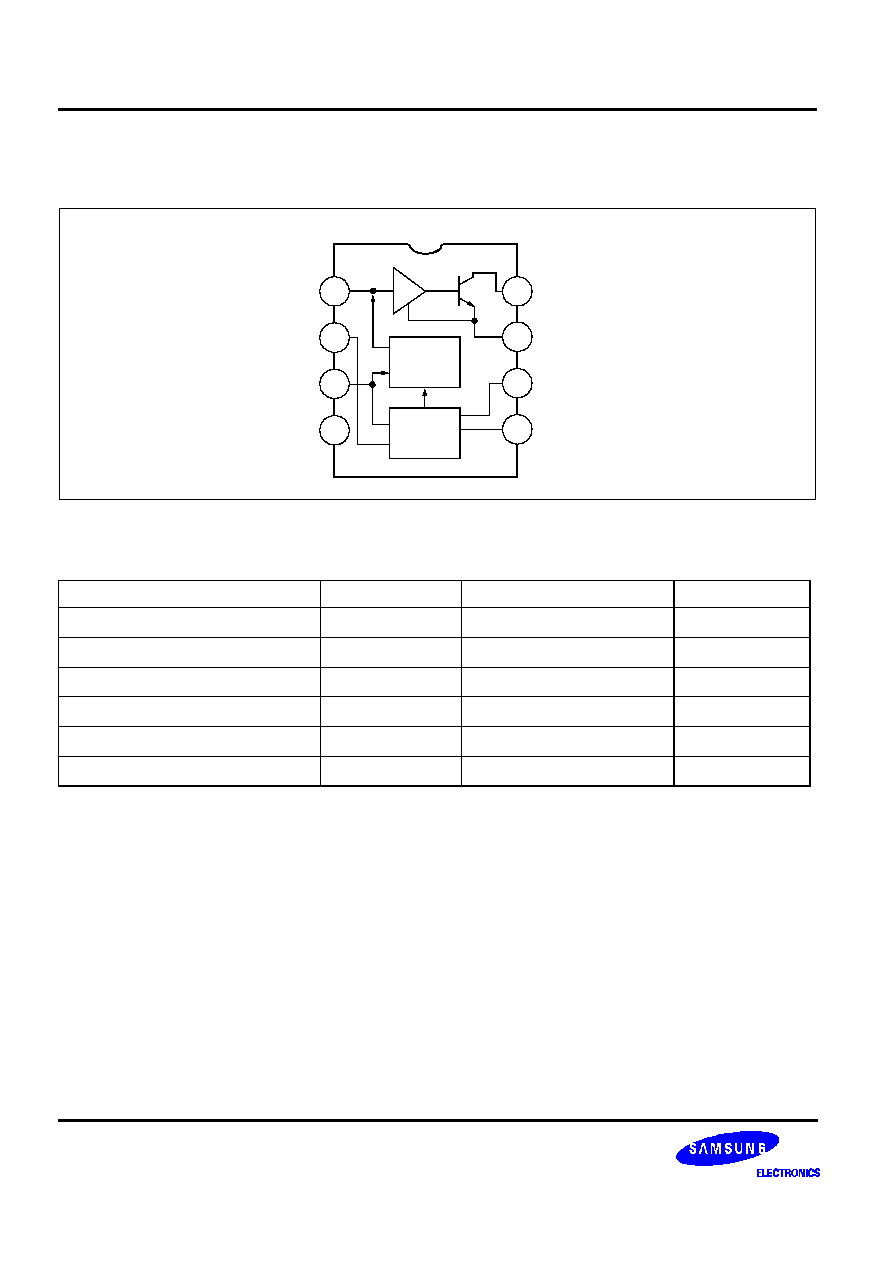
BLOCK DIAGRAM
ABSOLUTE MAXIMUM RATINGS
Characteristic
Symbol
Value
Unit
Supply Voltage
V
CC
10
V
Input Voltage
V
I
-
10 -- V
CC
+ 0.5
V
Output Voltage
V
O
15
V
Power Dissipation
P
D
300
mW
Operating Temperature
T
OPR
0 -- + 70
∞
C
Storage Temperature
T
STG
-
65 -- + 150
∞
C
1
2
3
4
5
6
7
8
OUTPUT
GND
TIMING CAPACITOR
TIMING RESISTOR
OUTPUT FILTER
LOOP FILTER
INPUT
Vcc
Amp.
Quadrature
Phase
Detector
Phase Locked
Loop
(PLL)

TONE DECODER
S1T
0567
3
ELECTRICAL CHARACTERISTICS
(V
CC
= 5.0 V, Ta = 25
∞
C unless otherwise specified)
Characteristic
Symbol
Test Conditions
Min.
Typ.
Max.
Unit
Operating voltage range
Operating current quiescent
Operating current activated
Quiescent power dissipation
V
CC
I
CC (Q)
I
CC (A)
P
D (Q)
R
L
= 20K
4.75
5.0
7
12
35
9.0
10
15
V
mA
mA
mW
High center frequency
Center frequency stability
Center frequency shift
with supply voltage
f
HC
f
ST
f
C
/
V
CC
R
L
= 20K
Ta = 0
∞
C to 70
∞
C
100
500
±
60
0.7
2
kHz
ppm/
∞
C
%/V
Largest detection bandwidth
Largest detection B.W skew
Largest detection bandwidth
variation with supply voltage
Largest detection bandwidth
variation with temperature
BW
DET
BW
DET
BW/
V
CC
BW/
T
-
10
14
2
±
2
±
0.1
18
3
±
5
% of fo
% of fo
%/V
%/
∞
C
Input Resistance
R
I
-
-
20
-
Kohm
Smallest detectable input voltage
Largest No output input voltage
V
I (SMALL)
V
I (LARGE)
I
L
= 100mA, fi = fo
10
20
15
25
mVrms
mVrms
Greatest simultaneous outband
signal to inband signal ratio
Minimum input signal to
wideband noise ratio
S1/SD
S2/SD
R
L
= 20K
V
IN
= 300mV
rms
fi = fo = 100 kHz
fi
1
= 140kHz
fi
2
= 60kHz
-
+6
-
6
-
dB
dB
Fastest On-Off cycling rate
Output leakage current
C
R (ON-OFF)
I
O (LKG)
R
L
= 20 K
V
IN
= 2 5mV
rms
-
fo/20
0.01
25
µ
A
Output saturation voltage
V
SAT1
V
SAT2
I
L
= 300mA, V
IN
= 25mVrms
I
L
= 100mA, V
IN
= 25mVrms
-
0.2
0.6
0.4
1.0
V
V
Output fall time
Output rise time
t
F
t
R
R
L
= 50
R
L
= 50
-
30
150
-
nS
nS

S1T0567
TONE DECODER
4
TEST CIRCUIT
NOTE: Adjust for fo =100kHz
APPLICATION INFORMATION
CIRCUIT DESCRIPTION
The S1T0567 monolithic tone decoder consists of a phase detector, low pass filter, and current-controlled oscillator
which comprise the basic phase-locked loop, plus an additional low pass filter and quadrature detector enabling
detection on in-band signals. The device normally has a high open collector output capable of sinking 100 mA.
The input signal is applied to Pin 3 (20k
nominal input resistance). Free running frequency is controlled by an RC
network at Pin 5 , Pin 6 and can typically reach 500kHz. A capacitor on Pin 1 serves as the output filter and
eliminates out-of-band triggering. PLL filtering is accomplished with a capacitor on Pin 2; bandwidth and skew are
also dependent upon the circuitry here. Bandwidth is adjustable from 0% to 14% of the center frequency. Pin 4 is
+V
CC
(4.75 to 9V nominal, 10V maximum); Pin 7 is ground; and Pin 8 is an open collector output, pull-down when
an inband signal triggers the device.
Definition of S1T0567 Parameters
Center Frequency f
O
f
O
is the free-running frequency of the C
L
controlled oscillator with no input signal. It is determined by resistor R
1
between pins 5 and 6. Capacitor C
1
from pin 6 to ground f
O
can be approximated by
where R
1
is in ohms and C
1
is in farads.
1
2
3
4
5
6
7
8
S1T0567
+5V
RL
C1
3.3nF
R1
2.4K
C3
C2
C1
0.005
0.01
1uF
0.02uF
Vin
+5V
fi = 100kHz
fo
R
1
C
1
1

TONE DECODER
S1T
0567
5
LARGEST DETECTION BANDWIDTH
The largest detection bandwidth is the largest frequency range within which an input signal above the threshold
voltage will cause a logical zero state at the output. The maximum detection bandwidth corresponds to the lock
range of the PLL.
Detection Bandwidth (BW)
The detection bandwidth is the frequency range centered about f
O
, within which an input signal larger than the
threshold voltage (typically 20 mVrms) will cause a logic zero state at the output. The detection bandwidth
corresponds to the capture range of the PLL and is determined by the Iow-pass filter. The bandwidth of the filter,
as a percent of f
O
, can be determined by the approximation
where V
i
, is the input signal in volts, rms, and C
2
is the capacitance at pin 2 in
µ
F.
Detection Band Skew
The detection band skew is a measure of how accurately the largest detection band is centered about the center
frequency, f
O
. It is defined as (f
max
+ f
min
- 2f
O
)/f
O
, where f
max
and f
min
, are the frequencies corresponding to the
edges of the detection band. If necessary, the detection band skew can be reduced to zero by an optional centering
adjustment.
PIN DESCRIPTION
Output Filter-C
3
(Pin 1)
Capacitor C
3
connected from pin 1 to ground forms a simple low-pass post detection filter to eliminate spurious
outputs due to out-of-band signals. The time constant of the filter can be expressed as T
3
= R
3
C
3
, where R
3
(4.7k
)
is the internal impedance at pin 1.
The precise value of C
3
is not practical for most applications. To eliminate the possibility of false triggering by
spurious signals, it is recommended that C
3
be
2 C
2
. where C
2
is the loop filter capacitance at pin 2.
If the value of C
3
becomes too large, the turn-on or turn-off time of the output stage will be delayed until the voltage
change across C
3
reaches the threshold voltage. In certain applications, the delay may be desirable as a means of
suppressing spurious outputs. Conversely, if the value of C
3
is too small, the beat rate at the output of the
quadrature detector may cause a false logic level change at the output. (Pin 8)
The average voltage (during lock) at pin 1 is a function of the inband input amplitude in accordance with the given
transfer characteristic.
Loop Filter - C
2
(Pin 2)
Capacitor C
2
connected from pin 2 to ground serves as a single pole, low-pass filter for the PLL portion of the
S1T0567.
The filter time constant is given by T
2
= R
2
C
2
. where R
2
(10k
) is the impedance at pin 2.
The selection of C
2
is determined by the detection bandwidth requirements. For additional information see the sec-
tion on
"
Definition of S1T0567 Parameters
"
.
The voltage at pin 2, the phase detector output, is a linear function of frequency over the range of 0.95 to 1.05 f
O
,
with a slope of approximately 20 mV/% frequency deviation.
BW
1070
V
I
f
o
C
2
------------
=

S1T0567
TONE DECODER
6
Input (Pin 3)
The input signal is applied to pin 3 through a coupling capacitor. This terminal is internally biased at a DC level 2
volts above ground, and has an input impedance level of approximately 20k
.
Timing Resistor R
1
and Capacitor C
1
(Pins 5 and 6)
The center frequency of the decoder is set by resistor R
1
between pins 5 and 6, and capacitor C
1
from pin 6 to
ground, as shown in Figure 1.
Pin 5 is the oscillator squarewave output which has a magnitude of approximately V
CC
- 1.4V and an average DC
level of V
CC
/2. A 1 k
load may be driven from this point. The voltage at pin 6 is an exponential triangle waveform
with a peak-to-peak amplitude of 1 volt and an average DC level of V
CC
/2. Only high impedance loads should be
connected to pin 6 to avoid disturbing the temperature stability or duty cycle of the oscillator.
Logic Output (Pin 8)
Terminal 8 provides a binary logic output when an input signal is present within the pass-band of the decoder. The
logic output is an uncommitted, base-collector power transistor capable of switching high current loads. The current
level at the output is determined by an external load resistor R
L
, connected from pin 8 to the positive supply.
When an inband signal is present, the output transistor at pin 8 saturates with a collector voltage less than 1 volt
(typically 0.6V) at full rated current of 100mA. If large output voltage swings are needed, R
L
can be connected to a
supply voltage, V+, higher than the V
CC
supply. For safe operation, V+
20 volts.
OPERATING INSTRUCTIONS
SELECTION OF EXTERNAL COMPONENTS
A typical connection diagram for S1T0567 is shown in Figure 1. For most applications, the following procedure will
be sufficient for determination of the external components R
1
, C
1
, C
2
, and C
3
.
1. R
1
and C
1
should be selected for the desired center frequency by the expression f
O
=1/R
1
C
1
. For optimum
temperature stability, R
1
should be selected so that 2 K
and the R
1
C
1
product have sufficient stability over the
projected operating temperature range.
2. C
2
is a low-pass capacitor.
If the input amplitude variation is known, the required f
O
C
2
product can be found to give the desired bandwidth.
Capacitor C
2
connected from pin 2 to ground serves as a single pole, low-pass filter for the PLL portion of the
S1T0567 solely by the f
O
C
2
product.
3. Capacitor C
3
sets the band edge of the low-pass filter which attenuates frequencies outside of the detection
band and thereby eliminates spurious outputs. If C
3
is too small, frequencies adjacent to the detection band may
switch the output stage off and on at the beat frequency, or the output may pulse off and on during the turn-on
transient. A typical minimum value of C
3
is 2 C
2
.
Conversely, if C
3
is too large, turn-on and turn-off of the output stage will be delayed until the voltage across C
3
passes the threshold value.

TONE DECODER
S1T
0567
7
PRINCIPLE OF OPERATION
The S1T0567 is a frequency selective tone decoder system based on the phase-locked loop (PLL) principle. The
system is comprised of a phase-locked loop, a quadrature AM detector, a voltage comparator, and an output logic
driver. The four sections are internally interconnected as shown in block diagram.
When an input tone is present within the pass-band of the circuit, the PLL synchronizes or
"
locks
"
on the input
signal. The quadrature detector serves as a lock indicator : when the PLL is locked on an input signal, the DC
voltage at the output of the detector is shifted. This DC level shift is then converted to an output logic pulse by the
amplifier and logic driver. The logic driver is a
"
bare collector
"
transistor stage capable of switching 100mA loads.
The logic output at pin 8 is normally in a
"
high
"
state, until a tone that is within the capture range of the decoder is
present at the input. When the decoder is locked on an input signal, the logic output at pin 8 goes to a
"
low
"
state.
The center frequency of the detector is set by the free-running frequency of the current-controlled oscillator in the
PLL.
This free-running frequency, f
O
, is determined by the selection of R
1
and C
1
connected to pins 5 and 6, as shown in
Figure 1. The detection bandwidth is determined by the size of the PLL filter capacitor, C
2
; and the output response
speed is controlled by the output filter capacitor, C
3
.

S1T0567
TONE DECODER
8
NOTES