LB11990W
No. 6216-1/14
LB11990W
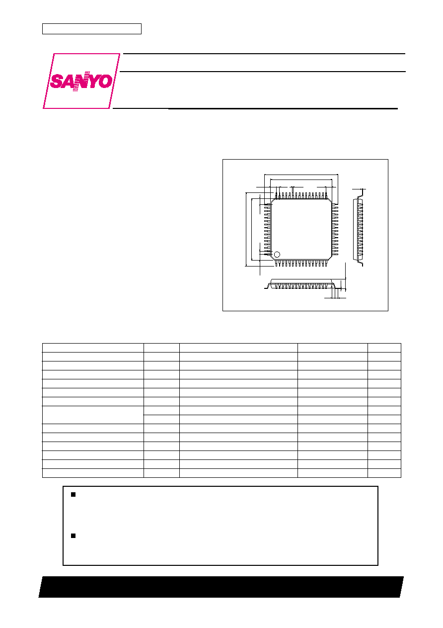
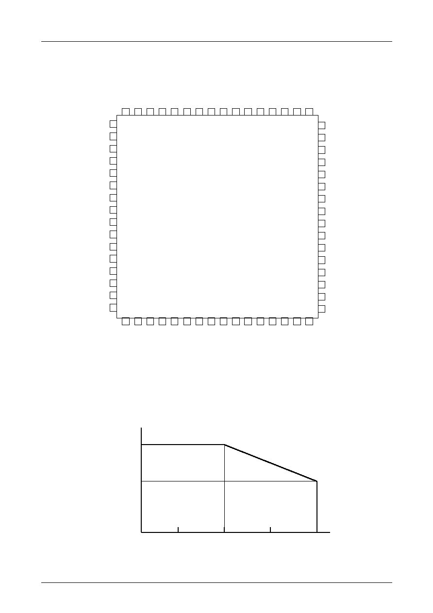
Package Dimensions
unit: mm
3190-SQFP64
Any and all SANYO products described or contained herein do not have specifications that can handle
applications that require extremely high levels of reliability, such as life-support systems, aircraft's
control systems, or other applications whose failure can be reasonably expected to result in serious
physical and/or material damage. Consult with your SANYO representative nearest you before using
any SANYO products described or contained herein in such applications.
SANYO assumes no responsibility for equipment failures that result from using products at values that
exceed, even momentarily, rated values (such as maximum ratings, operating condition ranges, or other
parameters) listed in products specifications of any and all SANYO products described or contained
herein.
N0199RM(KI)
Ordering number : ENN6216A
SANYO Electric Co.,Ltd. Semiconductor Company
TOKYO OFFICE Tokyo Bldg., 1-10, 1 Chome, Ueno, Taito-ku, TOKYO, 110-8534 JAPAN
Monolithic Digital IC
Three-Phase Brushless Motor Driver
[LB11990W]
SANYO : SQFP64
Specifications
Absolute Maximum Ratings
at Ta = 25
�
C
Parameter
Symbol
Conditions
Ratings
Unit
Maximum supply voltage 1
V
CC
1 max
7
V
Maximum supply voltage 2
V
CC
2 max
8.5
V
Maximum supply voltage 3
VS_C max Capstan motor driver
7.0
V
Maximum supply voltage 4
VS_D max Drum motor driver
7.0
V
Maximum supply voltage 5
VS_L max Loading motor driver
7.0
V
Applied output voltage
Vo max
8.0
V
Applied input voltage
VI1 max
Control circuits
�0.3 to V
CC
1 + 0.3
V
VI2 max
U, V, W, COM
8.0
V
Capstan motor output current
IOC max
1.0
A
Drum motor output current
IOD max
1.0
A
Loading motor output current
IOL max
0.6
A
Allowable power dissipation
Pd max
IC only
0.6
W
Operating temperature
Topr
�20 to +75
�
C
Storage temperature
Tstg
�55 to +150
�
C
10.0
12.0
1.25
0.5
1.25
1.25
0.5
1.25
0.18
12.0
1
16
17
32
33
48
49
64
10.0
0.5
1.7max
0.5
0.1
0.15
LB11990W
No. 6216-2/14
Electrical Characteristics/Capstan Motor Driver Block
at Ta = 25�C, V
CC
1 = 3V, V
CC
2 = 4.75V, V
S
= 1.5V
Parameter
Symbol
Conditions
Ratings
Unit
min
typ
max
Vcc1 power supply current
Icc1
Iout = 100 mA VSTBY_C = 3V
4
8
mA
Vcc2 power supply current
Icc2
Iout = 100 mA VSTBY_C = 3V
6
12
mA
Vcc1 idle current
Icc1Q
VSTBY_C = 0V
2.1
4
mA
Vcc2 idle current
Icc2Q
VSTBY_C = 0V
100
�
A
Vs idle current
IsQ
VSTBY_C = 0V
75
100
�
A
Upper side residual voltage
VXH1
Iout = 0.2A
0.15
0.22
0.29
V
Lower side residual voltage
VXL1
Iout = 0.2A
0.15
0.20
0.25
V
Upper side residual voltage
VXH2
Iout = 0.5A
0.25
0.40
V
Lower side residual voltage
VXL2
Iout = 0.5A
0.25
0.40
V
Output saturation voltage
Vosat
Iout = 0.8A, Sink + Source
1.40
V
Overlap amount
O.L
RL = 39
�
3, Rangle = 20 k
Note 2
73
80
87
%
Input offset voltage
VHOFF
Note 1 Design target value
�5
+5
mV
Common mode input range
VHCM
Rangle = 20 k
0.95
2.1
V
Input/output voltage gain
VGVH
Rangle = 20 k
24.5
27.5
30.5
dB
High level voltage
VSTH
2.5
V
CC
1
V
Low level voltage
VSTL
�0.2
+0.7
V
Input current
ISTIN
VSTBY_C = 3V
50
�
A
Leakage current
ISTLK
VSTBY_C = 0V
�30
�
A
High level voltage
VFRCH
2.5
V
CC
1
V
Low level voltage
VFRCL
�0.2
+0.4
V
Input current
IFRCIN
VFRC_C = 3V
20
30
�
A
Leakage current
IFRCLK
VFRC_C = 0V
�30
�
A
Hall power supply voltage
VHALL
IH = 5 mA, VH(+) � VH(�)
0.75
0.85
0.95
V
(�) pin voltage
VH(�)
IH = 5 mA
0.81
0.88
0.95
V
Input offset voltage
VFGOFF
�3
+3
mV
Input bias current
IbFG
VFGIN+ = VFGIN� = 1.5V
500
nA
Input bias current offset
IbFG
VFGIN+ = VFGIN� = 1.5V
�100
+100
nA
Common mode input range
VFGCM
1.2
2.5
V
High level output voltage
VFGOH
With internal pull-up
2.8
V
Low level output voltage
VFGOL
With internal pull-up
0.2
V
Voltage gain
VGFG
Note 1 Design target value
100
dB
Output current (Sink)
IFGOs
At output pin "L"
5
mA
Note 1: Design target value, not measured
Note 2: The overlap amount specification is taken as the measurement specification.
Allowable Operating Ranges
at Ta = 25
�
C
Parameter
Symbol
Conditions
Ratings
Unit
Power supply voltage 1
V
CC
1
V
CC
1
V
CC
2
2.7 to 6.0
V
Power supply voltage 2
V
CC
2
3.5 to 8.5
V
Power supply voltage 3
VS_C
VS_C
V
CC
2
to 7.0
V
Power supply voltage 4
VS_D
VS_D
V
CC
2
to 7.0
V
Power supply voltage 5
VS_L
VS_L
V
CC
2
2.2 to 7.0
V
Hall input amplitude
VHALL
Capstan motor
�
20 to
�
80
mVp�p
Power supply current
VX1
VX2
Hall amplifier
Standby pin
FRC pin
VH
FG comparator
LB11990W
No. 6216-3/14
Cylinder Motor Driver Block
at Ta = 25
�
C, V
CC
1 = 3V, V
CC
2 = 4.75V, V
S
= 3V
Parameter
Symbol
Conditions
Ratings
Unit
min
typ
max
Power supply current 4
ICC2
IO = 76 mA VSTBY_D = 3V VSTBY_C = 0V
0.75
2.5
mA
Output idle current 4
ICC2Q
VSTBY D = VSTBY_C = 0V
100
�
A
Output idle current 5
IS(D)Q
VSTBY D = VSTBY_C = 0V
100
300
�
A
Output saturation voltage, upper side 1
VOU1
IO = 0.1A RF = 0.25
0.3
0.5
V
Output saturation voltage, lower side 1
VOD1
IO = 0.1A RF = 0.25
0.3
0.5
V
Output saturation voltage, upper side 2
VOU2
IO = 0.4A, VS = 3V RF = 0.25
0.5
0.8
V
Output saturation voltage, lower side 2
VOD2
IO = 0.4A, VS = 3V RF = 0.25
0.5
0.8
V
COM pin common mode input voltage range
VIC
0.3
V
CC
2�0.9
V
Standby pin High level voltage
VSTBYH
2
V
CC
1
V
Standby pin Low level voltage
VSTBYL
�0.2
+0.7
V
Standby pin input current
ISTBYH
VSTBY_D = 3V
50
�
A
Standby pin leakage current
ISTBYL
VSTBY_D = 0V
�10
�
A
FRC pin High level voltage
VFRCH
2
V
CC
1
V
FRC pin Low level voltage
VFRCL
�0.2
+0.7
V
FRC pin input current
IFRCI
VFRC_D = 3V
50
�
A
FRC pin leakage current
IFRCL
VFRC_D = 0V
�10
�
A
Slope pin source current ratio
RSOURCE ICSLP1SOURCE/ICSLP2SOURCE
�15
+15
%
Slope pin sink current ratio
RSINK
ICSLP1SINK/ICSLP2SINK
�15
+15
%
CSLP1 source/sink current ratio
RCSLP1
ICSLP1SOURCE/ICSLP1SINK
�35
+15
%
CSLP2 source/sink current ratio
RCSLP2
ICSLP2SOURCE/ICSLP2SINK
�35
+15
%
Startup frequency
Freq
Cosc = 0.1
�
F, OSC frequency (Target)
11.5
Hz
Phase delay-width
Dwidth
(Target)
30
deg
SELCSLP pin High level voltage
VSELH
2
V
CC
1
V
SELCSLP pin Low level voltage
VSELL
�0.2
+0.7
V
SELCSLP pin input current
ISELH
VSELCSLP = 3V
50
�
A
SELCSLP pin leakage current
ISELL
VSELCSLP = 0V
�10
�
A
Note) Items shown to be "Target" are not measured.
FG/PG Amplifier Block
at Ta = 25
�
C, V
CC
1 = 3V, V
CC
2 = 4.75V, V
S
= 3V
Parameter
Symbol
Conditions
Ratings
Unit
min
typ
max
[FG amplifier]
Input offset voltage
VIO
(Target)
�
1
�
5
mA
Input bias current
IBIN�
(Target)
250
nA
Common mode input voltage range
VICOM
(Target)
1
2
V
Open loop gain
GVFG
f = 1 kHz (Target)
55
dB
Output ON voltage
VOL
At IO = 10
�
A
0.4
V
Output OFF voltage
VOH
At IO = 10
�
A
V
CC
1�0.5
V
Schmitt amplifier hysteresis width
VSHIS
(Target)
50
mV
Reference voltage
VREF
1.15
1.30
1.45
V
[PG amplifier]
Input offset voltage
VIO
(Target)
�
1
�
5
mV
Input bias current
IBIN�
(Target)
250
nA
Common mode input voltage range
VICOM
(Target)
1
2
V
Open loop gain
GVPG
f = 1 kHz (Target)
55
dB
Output ON voltage
VOL
At IO = 10
�
A
0.4
V
Output OFF voltage
VOH
At IO = 10
�
A
V
CC
1�0.5
V
Schmitt amplifier hysteresis width
VSHIS
(Target)
50
mV
Note) Items shown to be "Target" are not measured.
LB11990W
No. 6216-4/14
Loading Motor Driver Block
at Ta = 25
�
C, V
CC
1 = 3V, V
CC
2 = 4.75V, V
S
= 3V
Parameter
Symbol
Conditions
Ratings
Unit
min
typ
max
VCC1 power supply current 1
ICC11
VSTBY_C = VSTBY_D = 0V (standby)
2.1
4
mA
VCC1 power supply current 2
ICC12
VSTBY_C = VSTBY_D = 0V (forward/reverse)
14
19
mA
VCC1 power supply current 3
ICC13
VSTBY_C = VSTBY_D = 0V (at braking)
10
14
mA
VCC2 power supply current 1
ICC21
VSTBY_C, D = 0V (standby (V
CC
1 = OPEN))
100
�
A
VCC2 power supply current 2
ICC22
VSTBY_C, D = 0V (standby (V
CC
1 = 3.0V))
100
�
A
VCC2 power supply current 3
ICC23
VSTBY_C, D = 0V (forward/reverse)
15.0
25
mA
VS L power supply current
I VS L
VSTBY_C, D = 0V (standby)
20
�
A
[Logic input (DEC1 pin, DEC2 pin)]
High level input voltage
VINH
V
CC
1 = 2.7 to 4.0V
2.0
V
CC
1
V
High level flowing current
IINH
VIN = 3.0V
41
65
�
A
Low level input voltage
VINL
V
CC
1 = 2.7 to 4.0V
�0.2
0.6
V
Low level flowing current
IINL
VIN = 0.6V
5
10
�
A
[Loading motor driver]
Output saturation voltage 1
VOH
IO = 200 mA (upper/lower composition)
0.2
0.3
V
Output saturation voltage 2
VSHIS
IO = 400 mA (upper/lower composition)
0.4
0.6
V
[Reel FG amplifier]
Input offset voltage
VIO
�
1
�
5
mV
Input bias current
IB
1
�
A
Common mode input voltage range
VICM
1
2
V
Open loop gain
GV1
55
dB
[Thermal shutdown circuit]
TSD operating temperature
T-TSD
(Target)
180
�
C
TSD temperature hysteresis width
TSD
(Target)
15
�
C
Note) Items shown to be "Target" are not measured.
Truth Table
Capstan Motor Truth Table
Hall input
Source �> Sink
U
V
W
FRC
1
V �> W
H
H
L
H
W �> V
L
2
U �> W
H
L
L
H
W �> U
L
3
U �> V
H
L
H
H
V �> U
L
4
W �> V
L
L
H
H
V �> W
L
5
W �> U
L
H
H
H
U �> W
L
6
V �> U
L
H
L
H
U �> V
L
Note:
"H" for FR means a voltage of 2.50V or above. "L" for FR means a voltage of 0.4V or below.
(Vcc1 = 3V)
Note:
At the Hall input, "H" means that the potential of the (+) terminal for each phase input is at least 0.02V higher than the (�) terminal.
"L" means that the potential of the (+) terminal for each phase input is at least 0.02V lower than the (�) terminal.
Loading Motor Truth Table
Input
Output
Mode
DEC1
DEC2
OUT1
OUT2
L
L
Off
Off
Standby
H
L
H
L
Forward
L
H
L
H
Reverse
H
H
L
L
Brake
LB11990W
No. 6216-5/14
Pin Assignment
75
�20
25
50
0
0.6
0.36
0
Pd max � Ta
Ambient temperature, Ta [
�
C]
Power dissipation, Pd max [W]
RS_L
OUT2
RF_L
OUT1
VS_D
UOUT_D
VOUT_D
WOUT_D
RF_D
UOUT_C
NC
VOUT_C
WOUT_C
RF_C
UIN2
UIN1
FC1
OSC
FRC_D
FILTER
COM
VIN
FC2
VCC1
UIN
PGOUT_D
GND
WIN
PGC
FGIN_D
VREF
PGIN
STBY_D
BFGO
CSLP2
CSLP1
SELCSLP
RLM2
DEC1
STBY_C
NC
RLP1
RLM1
VS_L
DEC2
RLO1
RLO2
RLP2
FGIN1_D
FGIN2_D
VIN1
VIN2
WIN1
WIN2
VS_C
VH+
VH�
FRC_C
V
CC2
ANGLE
FGOUT_C
FGIN�
FGIN+
FGOUT_D
58
59
60
61
62
64
63
49
50
51
52
53
54
55
57
56
4
3
2
1
8
7
6
5
12
11
10
9
16
15
14
13
23
22
21
20
19
17
18
32
31
30
29
28
27
26
24
25
45
46
47
48
41
42
43
44
37
38
39
40
33
34
35
36
LB11990W
Top view