 | –≠–ª–µ–∫—Ç—Ä–æ–Ω–Ω—ã–π –∫–æ–º–ø–æ–Ω–µ–Ω—Ç: LC74732W | –°–∫–∞—á–∞—Ç—å:  PDF PDF  ZIP ZIP |
Ordering number : ENN
*
6526
63000RM (OT) No. 6526-1/38
Overview
The LC74731W and LC74732W are on-screen display
CMOS ICs that display characters and patterns on a TV
screen under the control of a microcontroller. These ICs
display 16
◊
16-dot characters and up to 12 lines of text
with 24 characters per line.
Features
∑ Text structure: 12 lines
◊
24 characters (Up to 288
characters)
∑ Character format: 16
◊
16 dots
Character display clock frequency: about 9 MHz
∑ Character sizes: Four sizes each in the horizontal and
vertical directions with the size set in line units.
∑ Number of characters supported:
LC74731W:256 (internal)
LC74732W:512 (internal)
Up to 8192 using an external ROM (for Japanese)
[Reference]
JIS X0298 (1990): 6877 characters
JIS level 1 kanji: 2965 characters
JIS level 2 kanji: 3388 characters
Special characters: 524 characters
∑ Display start positions: 128 positions each in the
horizontal and vertical directions
∑ Blinking, reverse video, reversed blinking, and character
outlining: May be specified in individual character units.
∑ Blinking types: Two types with periods of about 1.0 and
about 0.5 seconds.
∑ Blanking: The whole font area (16
◊
16 dots) can be
blanked in line units
(Four types: no blanking, character size blanking,
character plus outlining size blanking, and whole area up
to adjacent character blanking)
∑ Line spacing control: Zero to seven scan lines, in line
units
∑ Character color: Eight colors in character units (in
internal synchronization mode): 2 fsc and 4 fsc
(Black, red, green, yellow, blue, magenta, cyan, and
white)
∑ Character background color: Eight colors (in internal
synchronization mode): 2 fsc and 4 fsc
(Black, red, green, yellow, blue, magenta, cyan, and
transparent)
∑ Screen background color: Eight colors (in internal
synchronization mode): 2 fsc and 4 fsc
(Black, red, green, yellow, blue, magenta, cyan, and
white)
∑ External control inputs: Serial interface with an 8-bit
data size.
∑ Built-in sync separator circuit
∑ Video outputs: NTSC, PAL, PALM, PALN, NTSC
4.43, and PAL 60 composite video signal outputs
∑ Supports Y/C input
Package Dimensions
Preliminary
LC74731W,74732W
SANYO Electric Co.,Ltd. Semiconductor Company
TOKYO OFFICE Tokyo Bldg., 1-10, 1 Chome, Ueno, Taito-ku, TOKYO, 110-8534 JAPAN
On-Screen Display Controller
CMOS IC
Any and all SANYO products described or contained herein do not have specifications that can handle
applications that require extremely high levels of reliability, such as life-support systems, aircraft's
control systems, or other applications whose failure can be reasonably expected to result in serious
physical and/or material damage. Consult with your SANYO representative nearest you before using
any SANYO products described or contained herein in such applications.
SANYO assumes no responsibility for equipment failures that result from using products at values that
exceed, even momentarily, rated values (such as maximum ratings, operating condition ranges, or other
parameters) listed in products specifications of any and all SANYO products described or contained
herein.
10.0
12.0
1.25
0.5
1.25
1.25
0.5
1.25
0.18
12.0
1
16
17
32
33
48
49
64
10.0
0.5
1.7max
0.5
0.1
0.15
SANYO: SQFP64
[LC74731W,74732W]

Pin Assignment
No. 6526-2/38
LC74731W,74732W
1
V
SS
1
48
A6
2
XTALin
47
A7
3
XTALout
46
A8
4
CTRL1
45
A9
5
OSCin
44
A10
6
OSCout
43
A11
7
MUTE
42
A12
8
CDLR
41
A13
9
SYNCjdg/Rout
40
A14
10
CHARA/Gout
39
A15
11
BLANK/Bout
38
A16
12
IEOUT/BLKout
37
A17
13
OUTMOD
36
V
DD
1
14
CS
35
RST
15
SIN
(V)
34
SEPin
16
SCLK
33
SEPout
(H)
Cout
Cin
-NC-
-NC-
V
SS
2
-NC-
CVcr
SYNin
V
DD
2
-NC-
Cbias
Yout
Yin
CVout
CVin
HFTin
17
18
19
20
21
22
23
24
25
26
27
28
29
30
31
32
63
D1
62
D2
61
D3
60
D4
59
D5
58
D6
57
D7
56
CE
55
OE
54
A0
53
A1
52
A2
51
A3
50
A4
49
A5
64
D0
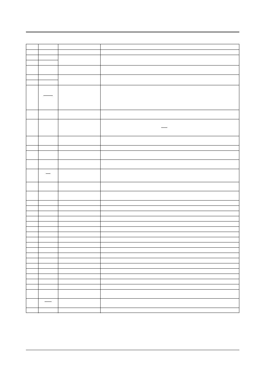
No. 6526-3/38
LC74731W,74732W
Pin Functions
Pin No.
Pin
Function
Description
1
V
SS
1
Ground
Ground connection. (Digital system ground)
2
Xtalin
Crystal oscillator connections
Connections for the crystal element and capacitors that form the internal sync signal generating
3
Xtalout
crystal oscillator. Xtalin can also be used to input an external clock signal. (2fsc or 4fsc)
4
CTRL1
Switches the crystal oscillator Selects external clock input mode or crystal oscillator mode. Low: crystal oscillator mode, high:
input
external clock input mode.
5
OSCin
LC oscillator connections
Connections for the coil and capacitor that form the character output dot clock generation oscillator.
6
OSCout
This is an active-low input with hysteresis characteristics (MORE+).
When low, the
7
MUTE
Muting control input
CVout, Yout, and Cout outputs are set to either,
(1) CSYNC,
CSYNC,
PE,
or
(2)
PE
PE,
PE.
In the initial state, (1) is selected. This setting is switched by commands.
8
CDLR
Background color phase
Connection for the resistor used to adjust the background color phase
adjustment
Outputs the result of the judgment as to whether or not the external sync signal is present.
9
SYNCJDG
External sync signal judgment A high level is output when a sync signal is present.
/Rout
output (Rout output)
The dot clock (LC oscillator) is output when RST is low.
(The IC can be set up to not output this signal during resets by commands.)
10
CHARA/Gout
Character output
Character signal output
(Gout output)
11
BLANK/Bout
Blank output (Bout output)
Blank signal output pin
12
IEout/BLKout
Internal/external output
Internal synchronization (high)/external synchronization (low) state output pin
(BLKout output)
13
OUTMOD
Output switching input
Switches between output from pins 9 to 12 and input to pin 32.
Low: normal operation, high: RGB output supported
Serial data input enable
14
CS
Enable input
Serial data input is enabled when low.
more+ (Hysteresis input characteristics)
15
SIN
Data input
Serial data input
more+ (Hysteresis input characteristics)
16
SCLK
Clock input
Serial data input clock input
more+ (Hysteresis input characteristics)
17
V
DD
2
Power supply
Composite video signal level adjustment power supply. (Analog system power supply)
18
COUT
Color signal output
Color (C) signal output
19
NC
This pin must either be left open or connected to ground.
20
CIN
Color signal input
Color (C) signal input
21
CBIAS
Chrominance bias output
Chrominance signal bias level output
22
NC
This pin must be either left open or connected to ground.
23
YOUT
Luminance signal output
Luminance signal (Y) output
24
NC
This pin must be either left open or connected to ground.
25
YIN
Luminance signal input
Luminance signal (Y) input
26
V
SS
2
Ground
Ground
27
CVOUT
Video signal output
Composite video signal output
28
NC
This pin must either be left open or connected to ground.
29
CVIN
Video signal input
Composite video signal input
30
CVCR
Video signal input
SECAM chrominance signal input
31
HFTin
Halftone signal input
Halftone signal input
32
SYNin
Sync separator circuit input
Video signal input to the internal sync separator circuit
33
SEPout
Composite sync signal output Composite sync signal output from the internal sync separator circuit
34
SEPin
Vertical sync signal input
Vertical sync signal input
MORE+ (Hysteresis input characteristics)
35
RST
Reset input
System reset input
A built-in pull-up resistor can be included in this pin's input circuit. (Hysteresis input characteristics)
36
V
DD
1
Power supply (+5 V)
Power supply (+5 V: digital system power supply)
Continued on next page.

No. 6526-4/38
LC74731W,74732W
Continued from preceding page.
Pin No.
Pin
Function
Description
37
A17
Address output 17
ROM address output 17
38
A16
Address output 16
ROM address output 16
39
A15
Address output 15
ROM address output 15
40
A14
Address output 14
ROM address output 14
41
A13
Address output 13
ROM address output 13
42
A12
Address output 12
ROM address output 12
43
A11
Address output 11
ROM address output 11
44
A10
Address output 10
ROM address output 10
45
A9
Address output 9
ROM address output 9
46
A8
Address output 8
ROM address output 8
47
A7
Address output 7
ROM address output 7
48
A6
Address output 6
ROM address output 6
49
A5
Address output 5
ROM address output 5
50
A4
Address output 4
ROM address output 4
51
A3
Address output 3
ROM address output 3
52
A2
Address output 2
ROM address output 2
53
A1
Address output 1
ROM address output 1
54
A0
Address output 0
ROM address output 0
55
OE
Output enable
ROM output enable output. This is an active-low output.
56
CE
Chip enable
ROM chip enable output. This is an active-low output.
57
D7
Data input 7
ROM data input 7. MORE+ (Hysteresis input characteristics)
58
D6
Data input 6
ROM data input 6. MORE+ (Hysteresis input characteristics)
59
D5
Data input 5
ROM data input 5. MORE+ (Hysteresis input characteristics)
60
D4
Data input 4
ROM data input 4. MORE+ (Hysteresis input characteristics)
61
D3
Data input 3
ROM data input 3. MORE+ (Hysteresis input characteristics)
62
D2
Data input 2
ROM data input 2. MORE+ (Hysteresis input characteristics)
63
D1
Data input 1
ROM data input 1. MORE+ (Hysteresis input characteristics)
64
D0
Data input 0
ROM data input 0. MORE+ (Hysteresis input characteristics)
No. 6526-5/38
LC74731W,74732W
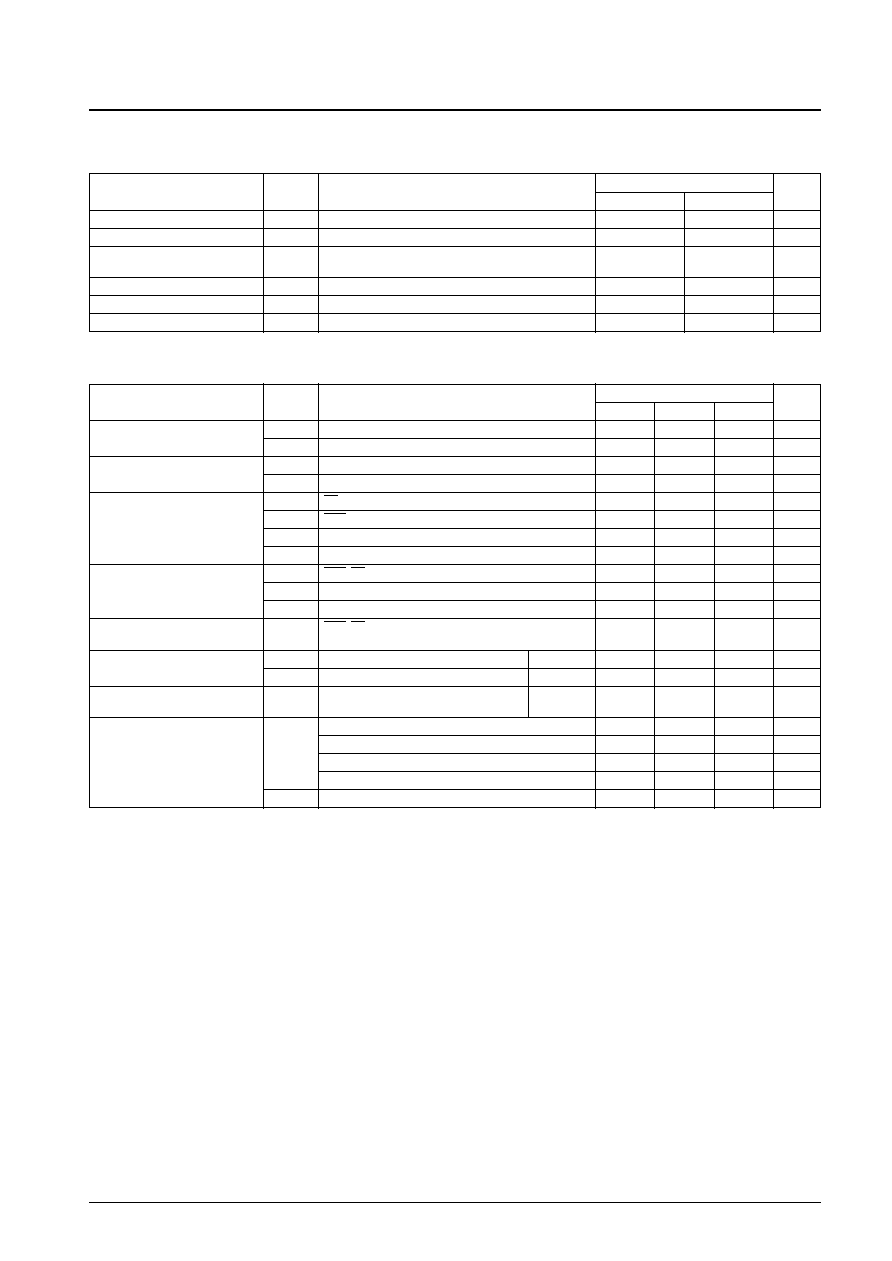
Specifications
Maximum Ratings
at Ta = 25∞C
Parameter
Symbol
Conditions
Ratings
Unit
min
max
Supply voltage
V
DD
V
DD
1 and V
DD
2
V
SS
≠ 0.3
V
SS
+ 6.5
V
Input voltage
V
IN
All input pins
V
SS
≠ 0.3
V
DD
1 + 0.3
V
Output voltage
V
OUT
SYNCJDG, BLANK, CHARA, SEPOUT, A0 to A17,
V
SS
≠ 0.3
V
DD
1 + 0.3
V
CE, and OE
Allowable power dissipation
Pdmax
--
275
mW
Operating temperature
Topr
≠30
+70
∞C
Storage temperature
Tstg
≠40
+125
∞C
Parameter
Symbol
Conditions
Ratings
Unit
min
typ
max
Supply voltage
V
DD
1
V
DD
1
4.5
5.0
5.5
V
V
DD
2
V
DD
2
4.5
5.0
6.5
V
Supply voltage
V
DD
1
V
DD
1
2.7
5.0
5.5
V
[Only for RGB output]
V
DD
2
V
DD
2
2.7
5.0
6.5
V
V
IH
1
CS, SIN, SCLK, SEPIN, and MUTE
0.8 V
DD
1
--
5.5
V
High-level input voltage
V
IH
2
RST
0.8 V
DD
1
--
V
DD
1 + 0.3
V
V
IH
3
CTRL1 and OUTMOD
0.7 V
DD
1
--
V
DD
1 + 0.3
V
V
IH
4
D0 to D7
0.8 V
DD
1
--
5.5
V
V
IL
1
RST, CS, SIN, SCLK, SEPIN, and MUTE
V
SS
≠ 0.3
--
0.2 V
DD
1
V
Low-level input voltage
V
IL
2
CTRL1 and OUTMOD
V
SS
≠ 0.3
--
0.3 V
DD
1
V
V
IL
3
D0 to D7
V
SS
≠ 0.3
--
0.2 V
DD
1
V
Pull-up resistor
R
PU
RST, CS, SIN, SCLK, and MUTE (when the pull-up
25
50
90
k
resistor option is specified)
Composite video signal input
V
IN
1
CVIN and CVCR
V
DD
1 = 5 V
--
2.0
--
Vp-p
voltage
V
IN
2
SYNIN
V
DD
1 = 5 V
1.5
2.0
2.5
Vp-p
Input voltage
V
IN
3
XtalIN (when an external clock input is used)
V
DD
1 = 5 V
--
--
5.0
Vp-p
fin = 2 fsc, 4 fsc
The XtalIN and XtalOUT oscillator pins (2 fsc: NTSC)
7.159
MHz
F
OSC1
The XtalIN and XtalOUT oscillator pins (4 fsc: NTSC)
14.318
MHz
Oscillator frequency
The XtalIN and XtalOUT oscillator pins (2 fsc: PAL)
--
8.867
--
MHz
The XtalIN and XtalOUT oscillator pins (4 fsc: PAL)
--
17.734
--
MHz
F
OSC2
The OSCin and OSCout oscillator pins (LC oscillator)
--
10
--
MHz
Recommended Operating Conditions
Note: If the Xtalin pin is used in clock input mode, applications must take adequate input noise prevention and reduction measures.