 | –≠–ª–µ–∫—Ç—Ä–æ–Ω–Ω—ã–π –∫–æ–º–ø–æ–Ω–µ–Ω—Ç: LC7930NW | –°–∫–∞—á–∞—Ç—å:  PDF PDF  ZIP ZIP |
LCD Drivers
Overview
The LC7930N, 7930NW are CMOS LSIs which incorporate
20-bit shift register, latch, and two sets of 20 LCD drivers.
They also have two switching pins: one of them (channel 2)
can be used as a scan-line driver (back plate) and the other
(channel 1) as a segment driver. They are optimal for LCD
interface with microcontroller (4 or 8 bits) or dot matrix
controller circuit incorporating character generator.
Features
.
Two channels of 20 output segment drivers
.
The configuration of 20 output segment drivers + 20
scanning terminal drivers available
.
A series data to connect with the microcontroller and three
control signals
.
Able to be connected in series for large display
.
Built-in bidirectional shift register can be shifted in the
direction that makes wiring easy
.
Operating supply voltage/ Operating temperature:
V
DD
= 4.5 to 5.5 V / Topr = ≠20 to +75∞C
.
Operating current drain : I
DD
= 1.0 mA max
(Logic = 400 kHz, LCD = 1 kHz)
.
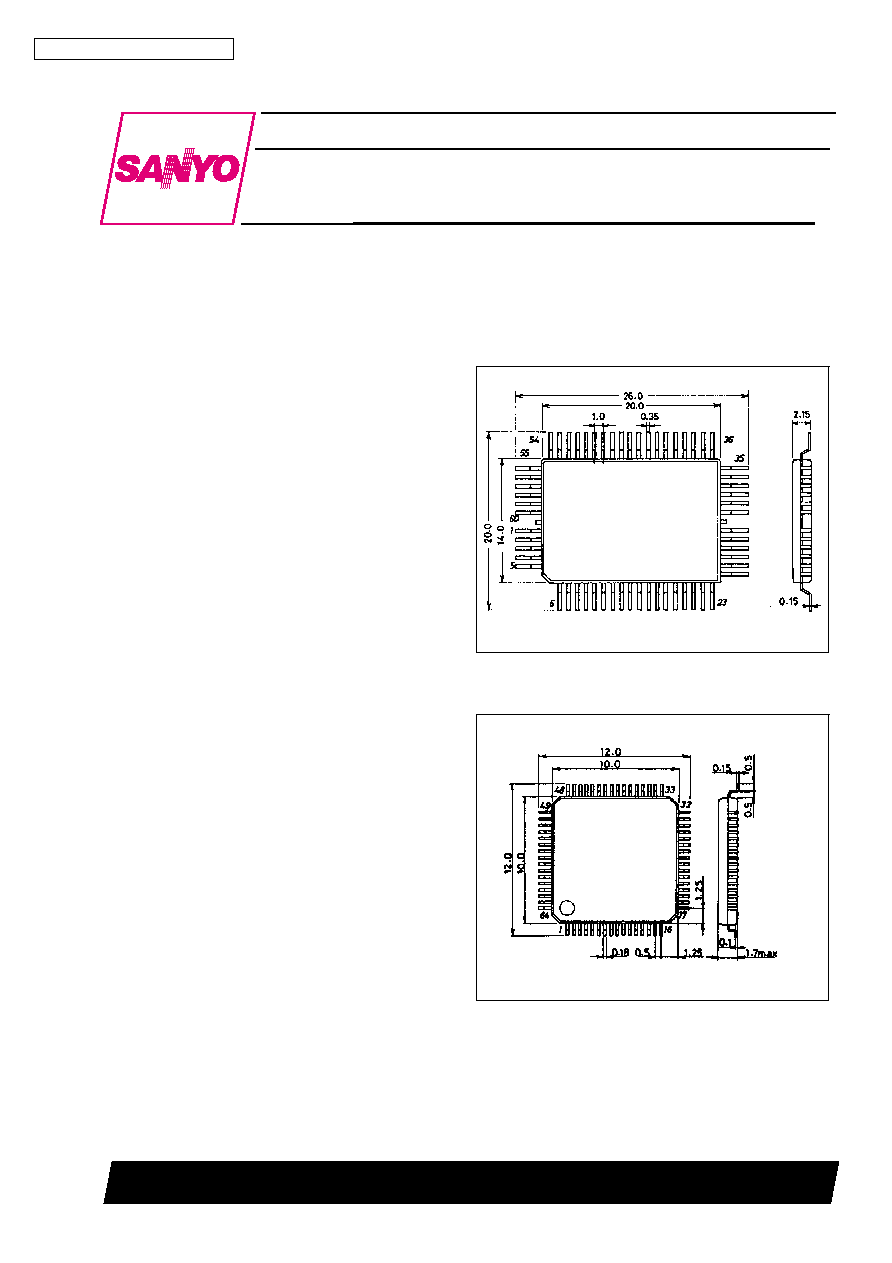
Package : Pin 60 Flat LC7930N : QIP60
Pin 64 Flat LC7930NW : SQFP64
Package Dimensions
unit : mm
3055A-QFP60C
[LC7930N]
SANYO : QIP60C
unit : mm
3190-SQFP64
[LC7930NW]
SANYO : SQFP64
Ordering number: EN2778C
CMOS LSI
LC7930N, 7930NW
SANYO Electric Co.,Ltd. Semiconductor Bussiness Headquarters
TOKYO OFFICE Tokyo Bldg., 1-10, 1 Chome, Ueno, Taito-ku, TOKYO, 110 JAPAN
13097HA(II)/12593JN/6031JN/6218TA,TS No.2778-1/7
Specifications
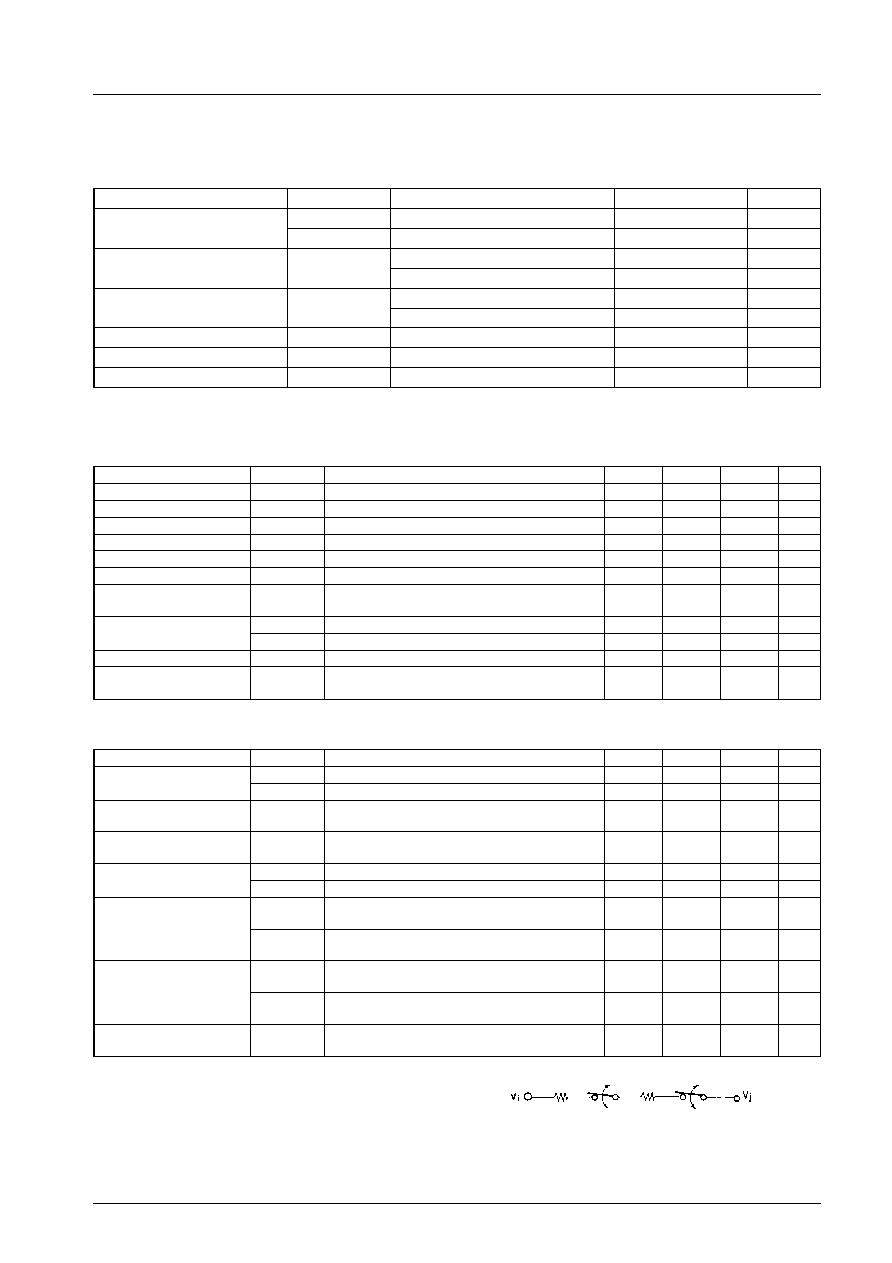
Absolute Maximum Ratings
at Ta = 25
±
2∞C
Parameter
Symbol
Conditions
Ratings
Unit
Maximum supply voltage
V
DD
max
≠0.3 to +7.0
V
V
EE
max
V
DD
≠13.5 to V
DD
+0.3
V
Maximum input voltage
V
I
max
≠0.3 to V
DD
+0.3
V
V1, V2, V3, V4, V5, V6
V
EE
to V
DD
+0.3
V
Maximum output voltage
V
O
max
≠0.3 to V
DD
+0.3
V
Output transistor OFF, Y1 to Y40
V
EE
to V
DD
+0.3
V
Allowable power dissipation
Pd max
100
mW
Operating temperature
Topr
≠20 to +75
∞C
Storage temperature
Tstg
≠55 to +125
∞C
Note : Don't soak the whole of IC into the tank filled with melted solder for soldering
Allowable Operating Conditions
at Ta = ≠20 to +75∞C, V
SS
= 0 V, V
EE
= ≠4 to ≠6 V
Parameter
Symbol
Conditions
min
typ
max
Unit
Supply voltage
V
DD
V
DD
4.5
5.5
V
High-level input voltage
V
IH
Note (1)
0.7V
DD
V
DD
V
Low-level input voltage
V
IL
Note (1)
V
SS
0.3V
DD
V
Shift frequency
f
CL
CLK
SR
400
kHz
High-level clock width
t
CWH
CLK
SR
, CLK
LA
800
ns
Low-level clock width
t
CWL
CLK
SR
800
ns
Data setup time
t
SU
LDATA1, LDATA2,
RDATA1, RDATA2
300
ns
Clock setup time
t
SL
CLK
SR
, CLK
LA
CLK
SR
CLK
LA
500
ns
t
LS
CLK
SR
, CLK
LA
CLK
LA
CLK
SR
500
ns
Clock transition time
t
ct
CLK
SR
, CLK
LA
200
ns
Data retention time
t
DH
LDATA1, LDATA2,
RDATA1, RDATA2
300
ns
Electirical Characteristics
at Ta = ≠20 to +75∞C, V
DD
= +5 V
±
10%, V
SS
= 0 V, V
EE
= ≠4 to ≠6 V
Parameter
Symbol
Conditions
min
typ
max
Unit
Input leakage current
I
IH
Note (1)
Vin = V
DD
5
µA
I
IL
Note (1)
Vin = V
SS
≠5
µA
High-level output voltage
V
OH
LDATA1, LDATA2,
RDATA1, RDATA2
I
OH
= ≠0.4 mA
V
DD
≠0.4
V
Low-level output voltage
V
OL
LDATA1, LDATA2,
RDATA1, RDATA2
I
OL
= 0.4 mA
0.4
V
Vi to Yj voltage down
V
d1
Y1 to Y40 Note (2)
Ion = 100 µA, single output
1.1
V
V
d2
Y1 to Y40 Note (2)
Ion = 50 µA, all outputs
1.5
V
Vi quiescent current
I
VH
V1 to V6
Open output pins
Vin = V
DD
10
µA
I
VL
V1 to V6
Open output pins
Vin = V
EE
≠10
µA
Supply current
I
DD
V
DD
Open output pins
CLK
SR
= 400 kHz
1.0
mA
I
EE
V
EE
Open output pins
M = 1 kHz
10
µA
Output propagation
delay time
t
PD
LDATA1, LDATA2,
RDATA1, RDATA2
C
L
= 15 pF
500
ns
Note (1): Applied to the pins; CLK
SR
, CLK
LA
, LDATA1, RDATA1, LDATA2, RDATA2, M, L/R1, L/R2, CH2-BP
(2): The equivalent circuit between Vi to Yj (i = 1 to 6, j = 1 to 40)
LC7930N, 7930NW
No.2778-2/7
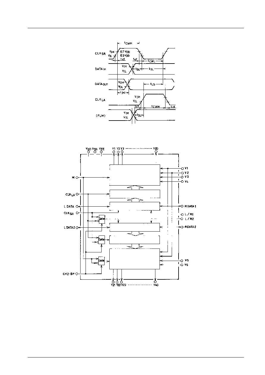
Switching Waveforms
Internal Equivalent Circuit
LCD driver
(Channel 1)
20-bit latch
20-bit bidirectional
shift register
20-bit bidirectional
shift register
20-bit latch
LCD driver
(Channel 2)
LC7930N, 7930NW
No.2778-3/7

Pin Assignment
[LC7930N]
Number
Name
Input/Output
Number
Name
Input/Output
Number
Name
Input/Output
1
Y30
Output
21
Y14
Output
41
RDATA1
Input/Output
2
Y31
Output
22
Y13
Output
42
LDATA2
Input/Output
3
Y32
Output
23
Y12
Output
43
RDATA2
Input/Output
4
Y33
Output
24
Y9
Output
44
N.C.
--
5
Y34
Output
25
Y10
Output
45
M
Input
6
Y29
Output
26
Y11
Output
46
L/R1
Input
7
Y28
Output
27
Y8
Output
47
L/R2
Input
8
Y27
Output
28
Y7
Output
48
CH2-BP
Input
9
Y26
Output
29
V
DD
--
49
V1
Input
10
Y25
Output
30
Y6
Output
50
V2
Input
11
Y24
Output
31
Y5
Output
51
V3
Input
12
Y23
Output
32
Y4
Output
52
V4
Input
13
Y22
Output
33
Y3
Output
53
V5
Input
14
Y21
Output
34
Y2
Output
54
V6
Input
15
Y20
Output
35
Y1
Output
55
Y40
Output
16
Y19
Output
36
V
EE
--
56
Y39
Output
17
Y18
Output
37
CLK
LA
Input
57
Y38
Output
18
Y17
Output
38
CLK
SR
Input
58
Y37
Output
19
Y16
Output
39
V
SS
--
59
Y36
Output
20
Y15
Output
40
LDATA1
Input/Output
60
Y35
Output
[LC7930NW]
Number
Name
Input/Output
Number
Name
Input/Output
Number
Name
Input/Output
1
V5
Input
23
Y6
Output
45
Y26
Output
2
V4
Input
24
V
DD
--
46
Y27
Output
3
V3
Input
25
Y7
Output
47
Y28
Output
4
V2
Input
26
Y8
Output
48
Y29
Output
5
V1
Input
27
Y11
Output
49
N.C.
--
6
CH2-BP
Input
28
Y10
Output
50
Y34
Output
7
L/R2
Input
29
Y9
Output
51
Y33
Output
8
L/R1
Input
30
Y12
Output
52
Y32
Output
9
M
Input
31
Y13
Output
53
Y31
Output
10
RDATA2
Input/Output
32
N.C.
--
54
Y30
Output
11
LDATA2
Input/OUtput
33
Y14
Output
55
N.C.
--
12
RDATA1
Input/Output
34
Y15
Output
56
N.C.
--
13
LDATA1
Input/Output
35
Y16
Output
57
Y35
Output
14
V
SS
--
36
Y17
Output
58
Y36
Output
15
CLK
SR
Input
37
Y18
Output
59
Y37
Output
16
CLK
LA
Input
38
Y19
Output
60
Y38
Output
17
V
EE
--
39
Y20
Output
61
Y39
Output
18
Y1
Output
40
Y21
Output
62
Y40
Output
19
Y2
Output
41
Y22
Output
63
V6
Input
20
Y3
Output
42
Y23
Output
64
N.C.
--
21
Y4
Output
43
Y24
Output
22
Y5
Output
44
Y25
Output
LC7930N, 7930NW
No.2778-4/7
Pin Descriptions
Pin Name
Function
V
DD
Logic circuitry power supply (+5 V
±
10%)
V
SS
0 V
V
EE
LCD driver power supply (≠4 to ≠6 V)
Y1 to Y20
Channel 1 LCD driver output pins
Y21 to Y40
Channel 2 LCD driver output pins
V1, V2
Reference voltage for selected driver outputs
V3, V4
Reference voltage for non-selected driver outputs (channel 1)
V5, V6
Reference voltage for non-selected driver outputs (channel 2)
L/R1
Shift direction for channel 1 shift register
L/R2
Shift direction for channel 2 shift register
LDATA1
RDATA1
Serial data input/output pins for channel 1 shift register
LDATA2
RDATA2
Serial data input/output pins for channel 2 shift register
M
Switching clock signal for LCD driver.
CLK
LA
Latches channael 1 data on the falling edge.
This also will latch channel 2 data on the falling edge if CH2-BP is low.
CLK
SR
Shift channel 1 data on the falling edge.
This also will shift channel 2 data on the falling edge if CH2-BP is low.
CH2-BP
Switches the mode of channel 2.
Exchanges the latch signal for the shift signal of channel 2 and invert the M signal.
Channel 2, then, can be used as a scan-line driver.
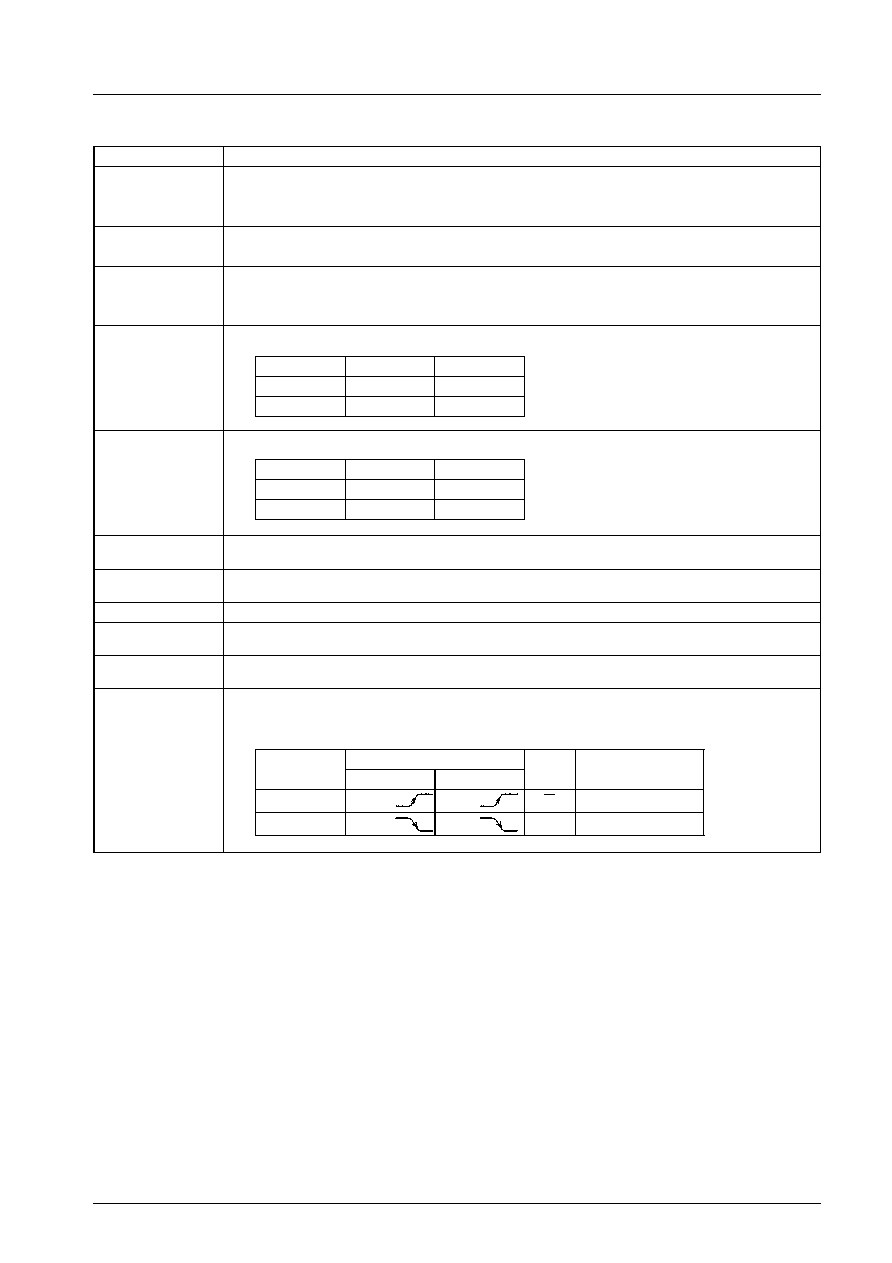
L/R1
LDATA1
RDATA1
High-level
Output
Input
Low-level
Input
Output
L/R2
LDATA2
RDATA2
High-level
Output
Input
Low-level
Input
Output
CH2-BP
Channel 2
M
Latch
Shift
High
CLK
SR
CLK
LA
M
For scan-line driver
Low
CLK
LA
CLK
SR
M
For signal line driver
Functional Description
LC7930N, LC7930NW are serial data transfer type LCD drivers.
Data inputted serially from the data pin is shifted successively by the synchronizing clock (CLK
SR
) and latched by the latch clock
(CLK
LA
) when the all data are shifted.
.
Segment terminal
When CH2-BP goes to low, the data of channel 1 and channel 2 are shifted at the falling edge of CLK
SR
, and then latched at
the falling edge of the CLK
LA
. The reference pulse will be switched to selected or unselected due to the latched data.
.
Scan terminal
When CH2-BP goes to high, the data of channel 2 is shifted at the rising edge of CLK
LA
, and then latched at the rising edge of
the CLK
SR
. When FLM signal, as a data, is inputted, the output will be scan terminal drive mode.
Continued on next page.
LC7930N, 7930NW
No.2778-5/7