 | –≠–ª–µ–∫—Ç—Ä–æ–Ω–Ω—ã–π –∫–æ–º–ø–æ–Ω–µ–Ω—Ç: LH1548 | –°–∫–∞—á–∞—Ç—å:  PDF PDF  ZIP ZIP |
Document Outline
- ˛ˇ
- ˛ˇ
- ˛ˇ
- ˛ˇ
- ˛ˇ
- ˛ˇ
- ˛ˇ
- ˛ˇ
- ˛ˇ
- ˛ˇ
- ˛ˇ
- ˛ˇ
- ˛ˇ
- ˛ˇ

In the absence of confirmation by device specification sheets, SHARP takes no responsibility for any defects that may occur in equipment using any SHARP devices shown in
catalogs, data books, etc. Contact SHARP in order to obtain the latest device specification sheets before using any SHARP device.
1
DESCRIPTION
The LH1548 is a 240-output segment driver IC
suitable for driving large/medium scale dot matrix
LCD panels, and is used in personal computers/
work stations. Through the use of UST (Ultra Slim
TCP) technology, it is ideal for substantially
decreasing the size of the frame section of the LCD
module. When combined with the LH1530 common
driver, it can create a low power consuming, high-
resolution LCD.
FEATURES
∑ Number of LCD drive outputs : 240
∑ Supply voltage for LCD drive : +10.0 to +42.0 V
∑ Supply voltage for the logic system : +2.5 to +5.5 V
∑ Shift clock frequency
≠ 25 MHz (Max.) : V
DD
= +5.0±0.5 V
≠ 15 MHz (Max.) : V
DD
= +3.0 to +4.5 V
≠ 12 MHz (Max.) : V
DD
= +2.5 to +3.0 V
∑ Low power consumption
∑ Low output impedance
∑ Adopts a data bus system
∑ 8-bit/12-bit parallel input modes are selectable
with a mode (MD) pin.
∑ Automatic transfer function of an enable signal
∑ Automatic counting function which, in the chip
selection mode, causes the internal clock to be
stopped by automatically counting 240 bits of
input data
∑ Package : 272-pin TCP (Tape Carrier Package)
PIN CONNECTIONS
LH1548
LH1548
240-output LCD Segment Driver IC
240
241
272
1
Y
239
Y
240
Y
238
Y
3
Y
2
Y
1
CHIP SURFACE
V
0R
V
2R
V
3R
V
5R
V
SS
TEST
2
TEST
1
MD
SHL
FR
EIO
1
LP
DISPOFF
XCK
DI
11
DI
10
DI
9
DI
8
DI
7
DI
6
DI
5
DI
4
DI
3
DI
2
DI
1
DI
0
EIO
2
V
DD
V
5L
V
3L
V
2L
V
0L
272-PIN TCP
TOP VIEW
NOTE :
Doesn't prescribe TCP outline.

LH1548
2
PIN DESCRIPTION
BLOCK DIAGRAM
PIN NO.
SYMBOL
I/O
DESCRIPTION
1 to 240
Y
1
-Y
240
O
LCD drive output
241, 272
V
0L
, V
0R
≠
Power supply for LCD drive
242, 271
V
2L
, V
2R
≠
Power supply for LCD drive
243, 270
V
3L
, V
3R
≠
Power supply for LCD drive
244, 269
V
5L
, V
5R
≠
Power supply for LCD drive
245
V
DD
≠
Power supply for logic system (+2.5 to +5.5 V)
246, 262
EIO
2
, EIO
1
I/O
Input/output for chip selection
247 to 258
DI
0
-DI
11
I
Display data input
259
XCK
I
Clock input for taking display data
260
I
Control input for output of non-select level
263
FR
I
AC-converting signal input for LCD drive waveform
266, 267
TEST
1
, TEST
2
I
Test mode selection input
V
0R
DI
0
DI
1
DI
2
DI
3
DI
4
DI
5
DI
6
DI
7
V
DD
V
SS
FR
EIO
1
EIO
2
LP
XCK
SHL
V
2R
V
3R
V
5R
Y
1
Y
2
Y
239
Y
240
SP CONVERSION & DATA CONTROL
(8 to 24 or 12 to 24)
TEST
CIRCUIT
DATA LATCH CONTROL
V
5L
V
3L
V
2L
V
0L
247
248
249
250
251
252
253
254
DI
8
255
DI
9
256
DI
10
257
DI
11
258
TEST
1
266
TEST
2
267
245
268
241
242
243
244
240
239
2
1
269
270
271
272
260
263
262
246
261
259
264
MD 265
LEVEL
SHIFTER
ACTIVE
CONTROL
CONTROL
LOGIC
240-BIT LINE LATCH
24 BITS x 2
DATA
LATCH
240-BIT LEVEL SHIFTER
240-BIT 4-LEVEL DRIVER
24
240
240
48
48
48
48
48
Ground (0 V)
≠
V
SS
268
Mode selection input
I
MD
265
Input for selecting the reading direction of display data
I
SHL
264
Latch pulse input for display data
I
LP
261

3
LH1548
BLOCK
FUNCTION
Active Control
Controls the selection or non-selection of the chip.
Following an LP signal input, and after the chip selection signal is input, a selection
signal is generated internally until 240 bits of data have been read in.
Once data input has been completed, a selection signal for cascade connection is
output, and the chip is non-selected.
SP Conversion &
Data Control
Data is retained until 24 bits have been completely input, after which they are put on the
internal data bus 24 bits at a time.
Data Latch Control
Selects the state of the data latch which reads in the data bus signals. The shift direction
is controlled by the control logic. For every 48 bits of data read in, the selection signal
shifts one bit based on the state of the control circuit.
Data Latch
Latches the data on the data bus. The latch state of each LCD drive output pin is
controlled by the control logic and the data latch control; 240 bits of data are read in 10
sets of 24 bits.
Line Latch
All 240 bits which have been read into the data latch are simultaneously latched at the
falling edge of the LP signal, and are output to the level shifter block.
Level Shifter
The logic voltage signal is level-shifted to the LCD drive voltage level, and is output to
the driver block.
4-Level Driver
Drives the LCD drive output pins from the latch data, and selects one of 4 levels (V
0
, V
2
,
V
3
or V
5
) based on the FR and
signals.
Control Logic
Controls the operation of each block. When an LP signal has been input, all blocks are
reset and the control logic waits for the selection signal output from the active control
block. Once the selection signal has been output, operation of the data latch and data
transmission is controlled, 240 bits of data are read in, and the chip is non-selected.
The circuit for testing. During normal operation, it isn't activated.
Test Circuit
FUNCTIONAL OPERATIONS OF EACH BLOCK
4
LH1548
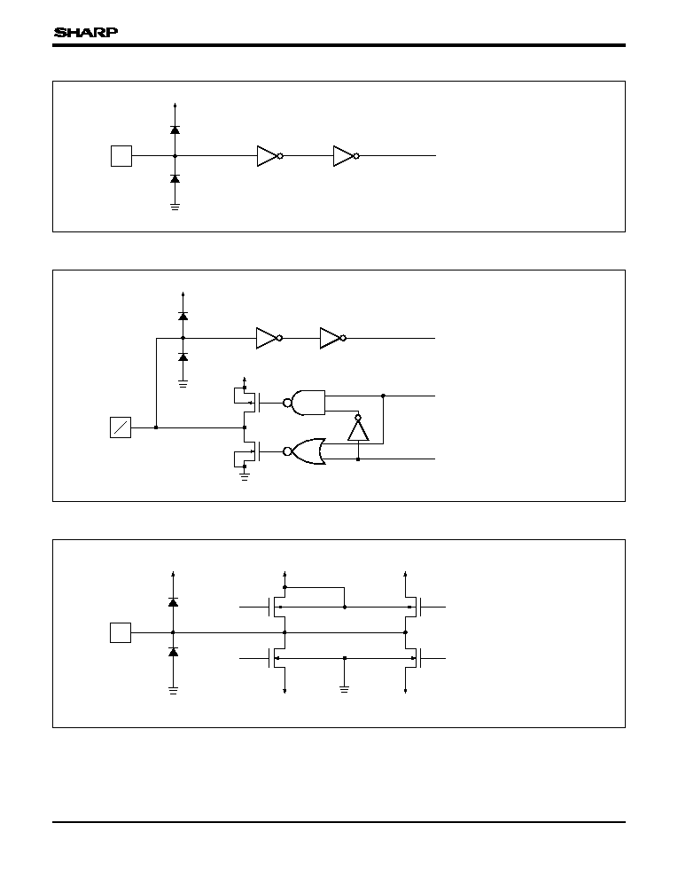
INPUT/OUTPUT CIRCUITS
I
V
DD
V
SS
(0 V)
To Internal Circuit
Fig. 1 Input Circuit
I
O
V
DD
V
SS
(0 V)
V
SS
(0 V)
To Internal Circuit
Output Signal
Control Signal
V
DD
Fig. 2 Input/Output Circuit
V
0
V
0
V
SS
(0 V)
V
2
V
SS
(0 V)
V
3
V
5
Control Signal 1
Control Signal 2
Control Signal 4
Control Signal 3
O
Fig. 3 LCD Drive Output Circuit
øApplicable pins°
DI
11
-DI
0
, XCK, LP, SHL,
FR, MD,
,
TEST
1
, TEST
2
øApplicable pins°
EIO
1
, EIO
2
øApplicable pins°
Y
1
-Y
240

5
LH1548
FUNCTIONAL DESCRIPTION
Pin Functions
SYMBOL
FUNCTION
V
DD
Logic system power supply pin, connected to +2.5 to +5.5 V.
V
SS
Ground pin, connected to 0 V.
V
0L
, V
0R
V
2L
, V
2R
V
3L
, V
3R
V
5L
, V
5R
Bias power supply pins for LCD drive voltage
∑ Normally use the bias voltages set by a resistor divider.
∑ Ensure that voltages are set such that V
SS
V
5
< V
3
< V
2
< V
0
.
∑ V
iL
and V
iR
(
i
=
0
,
2
,
3
,
5
) aren't connected with inside IC. Therefore, it is necessary that
these pins connect with an external power supply.
DI
11
-DI
0
Input pins for display data
∑ In 8-bit parallel input mode, input data into the 8 pins, DI
7
-DI
0
. Connect DI
11
-DI
8
to V
SS
or V
DD
.
∑ In 12-bit parallel input mode, input data into the 12 pins, DI
11
-DI
0
.
∑ Refer to
"RELATIONSHIP BETWEEN THE DISPLAY DATA AND LCD DRIVE OUTPUT
PINS"
in Functional Operations.
XCK
Clock input pin for taking display data
∑ Data is read at the falling edge of the clock pulse.
LP
Latch pulse input pin for display data
∑ Data is latched at the falling edge of the clock pulse.
SHL
Input pin for selecting the reading direction of display data
∑ When set to V
SS
level "L", data is read sequentially from Y
240
to Y
1
.
∑ When set to V
DD
level "H", data is read sequentially from Y
1
to Y
240
.
∑ Refer to
"RELATIONSHIP BETWEEN THE DISPLAY DATA AND LCD DRIVE OUTPUT
PINS"
in Functional Operations.
Control input pin for output of non-select level
∑ The input signal is level-shifted from logic voltage level to LCD drive voltage level, and
controls the LCD drive circuit.
∑ When set to V
SS
level "L", the LCD drive output pins (Y
1
-Y
240
) are set to level V
5
.
∑ Table of truth values is shown in
"TRUTH TABLE"
in Functional Operations.
FR
AC signal input pin for LCD driving waveform
∑ The input signal is level-shifted from logic voltage level to LCD drive voltage level, and
controls the LCD drive circuit.
∑ Normally it inputs a frame inversion signal.
∑ The LCD drive output pins' output voltage levels can be set using the line latch output
signal and the FR signal.
∑ Table of truth values is shown in
"TRUTH TABLE"
in Functional Operations.
MD
Mode selection pin
∑ When set to V
SS
level "L", 8-bit parallel input mode is set.
∑ When set to V
DD
level "H", 12-bit parallel input mode is set.
∑ Refer to
"RELATIONSHIP BETWEEN THE DISPLAY DATA AND LCD DRIVE OUTPUT
PINS"
in Functional Operations.