 | –≠–ª–µ–∫—Ç—Ä–æ–Ω–Ω—ã–π –∫–æ–º–ø–æ–Ω–µ–Ω—Ç: SP7545J | –°–∫–∞—á–∞—Ç—å:  PDF PDF  ZIP ZIP |
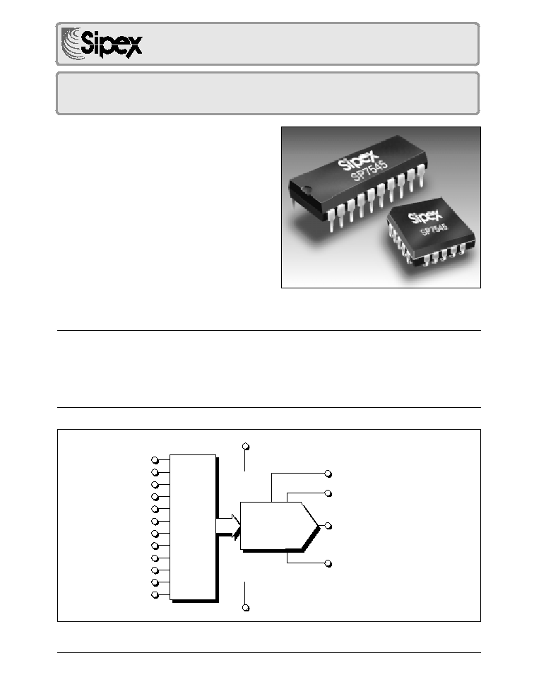
SP7545
12≠Bit, Buffered Multiplying DAC
© Copyright 2000 Sipex Corporation
1
DESCRIPTION...
The SP7545 is a low≠cost, high stability 12≠bit CMOS multiplying DAC with on≠board data
latches. The SP7545 is constructed using a proprietary low≠TCR thin≠film process that
requires no laser≠trimming to achieve 12≠bit performance. With no laser≠trimming, inherent
high stability, and a segmented (decoded) DAC architecture, the SP7545 retains its
performance over time and temperature. The SP7545 is available for use in commercial and
industrial temperature ranges. It is available in 20≠pin plastic DIP and PLCC packages.
s
±
1.0 LSB Relative Accuracy Over
Temperature
s
Monotonic to 12≠Bits Over
Temperature
s
High Stability, Segmented Architecture
s
Proprietary, Low TCR Thin≠Film
Resistor Technology
s
Operates With +5V to +15V Power
Supplies
s
On-Board, Level≠Triggered Latches
s
2kVESD Protection on all Digital
Inputs
D
11
(MSB) [4]
D
10
[5]
D
9
[6]
D
8
[7]
D
7
[8]
D
6
[9]
D
5
[10]
D
4
[11]
D
3
[12]
D
2
[13]
D
1
[14]
D
0
(LSB) [15]
12≠BIT
DAC
REGISTER
V
REF
[19]
R
FB
[20]
I
O1
[1]
AGND [2]
12≠BIT
DAC
V
DD
[18]
GND [3]
Æ
SP7545
12≠Bit, Buffered Multiplying DAC

SP7545
12≠Bit, Buffered Multiplying DAC
© Copyright 2000 Sipex Corporation
2
ABSOLUTE MAXIMUM RATINGS
(T
A
= 25
∞
C unless otherwise noted.)
These are stress ratings only and functional operation of the device
at these or any other above those indicated in the operation
sections of the specifications below is not implied. Exposure to
absolute maximum rating conditions for extended periods of time
may affect reliability.
V
DD
to GND .................................................................. ≠0.3V, +17V
Digital Input Voltage to GND ................................. ≠0.3V, V
DD
+0.3V
V
REF
or V
RFB
to GND ................................................................
±
25V
Output Voltage (Pin 1, Pin 2) ................................ ≠0.3V, V
DD
+0.3V
Power Dissipation (Any Package to +75
∞
C) ........................ 450mW
Derates above 75
∞
C by ...................................................... 6mW/
∞
C
Dice Junction Temperature ................................................. +150
∞
C
Storage Temperature ............................................ ≠65
∞
C to +150
∞
C
Lead Temperature (Soldering, 60 seconds) ........................ +300
∞
C
SPECIFICATIONS
(T
A
=25
∞
C; V
DD
=+5V or +15V as noted; V
REF
= +10V; I
O1
= AGND = GND = 0V; unipolar unless otherwise noted.)
PARAMETER
MIN.
TYP.
MAX.
UNIT
CONDITIONS
STATIC PERFORMANCE
Resolution
12
Bits
Integral Non-Linearity
Note 6
≠J
±
2.0
LSB
Note 5; 11-bit relative accuracy
≠K
±
1.0
LSB
Note 5; 12-bit relative accuracy
Differential Non-Linearity
Note 7
≠J
±
4.0
LSB
Note 5; monotonic to 12-bits
≠K
±
1.0
LSB
Note 5; monotonic to 12-bits
Gain Error
Note 16
≠J
±
20
LSB
V
DD
= +5V; Note 5
±
25
LSB
V
DD
= +15V
≠K
±
10
LSB
V
DD
= +5V
±
15
LSB
V
DD
= +15V
Output Leakage Current
±
10
nA
At I
O1
(Pin 1); Note 5 and 17
AC PERFORMANCE CHARACTERISTICS
Output Amplifier HOS-050;
Note 10
Propagation Delay
300
ns
V
DD
= +5V; Note 11
250
ns
V
DD
= +15V; Note 11
Current Settling Time
2.0
µ
s
Full scale transition; Note 12
Output Capacitance
50
200
pF
WR, CS = 0V; data inputs V
DD
200
pF
Note 5; data inputs V
DD
25
70
pF
Data inputs 0V
70
pF
Note 5; data inputs 0V
Glitch Energy
250
nV-s
Note 13
Multiplying Feedthrough Error
2.0
mV
P-P
Measured at output I
O1
; Note 14
0.2
mV
P-P
Measured at output I
O1
; Note 15
STABILITY
Gain Error TC
±
1.0
±
2.0
ppm/
∞
C
±
2.0
ppm/
∞
C
Note 5
Integral Non-Linearity TC
±
0.1
±
1.0
ppm/
∞
C
±
1.0
ppm/
∞
C
Note 5
Differential Non-Linearity TC
±
0.1
±
1.0
ppm/
∞
C
±
1.0
ppm/
∞
C
Note 5
Power Supply Rejection
±
0.002
±
0.01
%/%
%/0.005% change in power
supply voltage
±
0.02
%/%
Note 5
REFERENCE INPUT
Input Resistance
7
10
15
K
Pin 19 to GND
Input Resistance TC
±
150
ppm/
∞
C
Voltage Range
±
25
Volts
Note 5 and 8

SP7545
12≠Bit, Buffered Multiplying DAC
© Copyright 2000 Sipex Corporation
3
SPECIFICATIONS (continued)
(T
A
=25
∞
C; V
DD
=+5V, V
REF
= +10V; I
O1
= AGND = GND = 0V; unipolar unless otherwise noted.)
PARAMETER
MIN.
TYP.
MAX.
UNIT
CONDITIONS
DIGITAL INPUTS
Logic Levels
V
IH
2.4
V
DD
Volts
V
DD
= +5V
2.4
Volts
V
DD
= +5V; Note 5
13.5
V
DD
Volts
V
DD
= +15V
13.5
Volts
V
DD
= +15V; Note 5
V
IL
-0.3
0.8
Volts
V
DD
= +5V
0.8
Volts
V
DD
= +5V; Note 5
-0.3
1.5
Volts
V
DD
= +15V
1.5
Volts
V
DD
= +15V; Note 5
Input Current
±
1.0
µ
A
V
IN
= 0V or V
DD
±
10
µ
A
Note 5 and 9
Input Capacitance
V
IN
= 0; Note 5 and 8
Bits 1--12
5
pF
WR, CS
20
pF
Coding
Unipolar
Binary
Bipolar
Offset Binary
POWER REQUIREMENTS
Supply Current
2.0
mA
All digital inputs V
IL
or V
IH
2.0
mA
Note 5; all digital inputs
V
IL
or V
IH
0.5
mA
Note 18
mA
Note 5 and 18
ENVIRONMENTAL AND MECHANICAL
Operating Temperature
Commercial
0
+70
∞
C
Industrial
-40
+85
∞
C
Storage Temperature
-65
+150
∞
C
Package
20≠pin Plastic DIP
20≠pin Plastic LCC
Notes and Cautions:
1.
Do not apply voltages higher than V
DD
or less than GND potential on any terminal other than V
REF
or V
RFB
.
2.
The digital inputs are diode-clamp protected against ESD damage. However, permanent damage may
occur on unprotected units from high-energy electrostatic fields. Keep units in conductive foam at all
times until ready to use.
3.
Use proper anti-static handling procedures.
4.
Stresses above those listed under "Absolute Maximum Ratings" may cause permanent damage to the
device. This is a stress rating only and functional operation at or above these specifications is not
implied. Exposure to the above maximum rated conditions for extended periods may affect device
reliability.
5.
From T
MIN
to T
MAX
.
6.
End-point linearity
7.
Differential Non-linearity is the deviation of an output step from the theoretical value of 1 LSB for any two
adjacent digital input codes.
8.
Guaranteed by design, but not production tested.
9.
Logic inputs are MOS gates. I
IN
typically is less than 1nA @ 25
∞
C.
10.
AC performance characteristics are included for design guidance only and are subject to sample testing
only.
11.
R
L
= 100
, C
EXT
= 13pF; all data inputs 0V to V
DD
or V
DD
to 0V; from 50% digital input change to 90% of
final analog output.
12.
Settling to
±
0.01% FSR (strobed); all data inputs 0V to V
DD
or V
DD
to 0V.
13.
V
REF
= 0V, DAC register alternatively loaded with all 0's and all 1's.
14.
V
REF
= 20V
P-P
; F = 10kHz sinewave.
15.
V
REF
= 20V
P-P
; F = 1kHz sinewave.
16.
Measured using internal feedback resistor with DAC loaded with all 1's.
17.
All digital inputs = 0V.
18.
All digital inputs 0V or V
DD.
SP7545
12≠Bit, Buffered Multiplying DAC
© Copyright 2000 Sipex Corporation
4
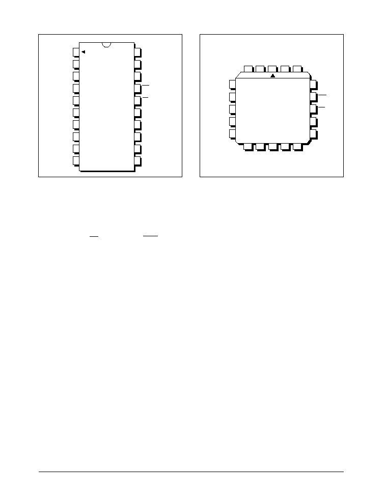
SP7545
I
01
AGND
GND
D
0
(MSB)
D
1
D
2
D
3
D
4
D
5
D
6
R
FB
V
REF
V
DD
WR
CS
D
11
(LSB)
D
10
D
9
D
8
D
7
1
2
3
4
5
6
7
8
9
10
20
19
18
17
16
15
14
13
12
11
GND
AGND
I
O1
R
FB
V
REF
SP7545
D
11
(MSB)
D
10
D
9
D
8
D
7
V
DD
WR
CS
D
0
(LSB)
D
1
D
6
D
5
D
4
D
3
D
2
18
17
16
15
14
9
10
11
12
13
3
2
1
20
19
4
5
6
7
8
PINOUT ≠ PLASTIC DIP
PINOUT ≠ PLASTIC LCC
FEATURES...
The SP7545 is a low≠cost, high stability 12≠bit
CMOS multiplying DAC with on≠board data
latches. The level≠triggered latch accepts a single
12≠bit wide data word under control of both
CHIP SELECT (CS) and WRITE (WR) control
line inputs. Tying both of these control lines low
makes the input latch transparent, allowing di-
rect, unbuffered operation of the DACs. The
SP7545 is ideally suited for applications requir-
ing stability over time and temperature, such as
digital gain blocks, attenuation control, robot-
ics, modems, medical and process instrumenta-
tion. Because of its low power dissipation, it is
also suited for battery≠powered equipment.
The SP7545 is constructed using a proprietary
low≠TCR thin≠film process that requires no
laser≠trimming to achieve 12≠bit performance.
With no laser≠trimming, inherent high stability,
and a segmented (decoded) DAC architecture,
the SP7545 retains its performance over time
and temperature. To further improve reliability,
the DAC features 2KV ESD protection on all
digital inputs. Each DAC is fully characterized
by all≠codes testing to eliminate any hidden
errors.
The SP7545 is available for use in commercial
and industrial temperature ranges. It operates
with power supply voltages from +5V to +15V.
It is available in 20≠pin plastic DIP and PLCC
packages.

SP7545
12≠Bit, Buffered Multiplying DAC
© Copyright 2000 Sipex Corporation
5
CHIP SELECT
WRITE
DATA IN
t
CS
t
WR
t
CH
t
DS
t
DH
DATA VALID
V
IH
V
IL
WRITE MODE:
CS and WR low, DAC responds to DATA INPUTS (D
0
≠D
11
).
HOLD MODE:
Either CS or WR high, DATA INPUTS are locked out; DAC holds
last data present when either CS or WR was asserted high.
TIMING
AC DYNAMICS
(T
A
=25
∞
C; V
DD
=+5V or +15V as noted, V
REF
= +10V; I
O1
= AGND = GND = 0V; unipolar unless otherwise noted.)
PARAMETER
MIN.
TYP.
MAX.
UNIT
CONDITIONS
Refer to Timing Diagram
t
CS
t
WR
,; t
CH
0
t
CS
-- Chip Select to Write Setup Time
280
200
ns
V
DD
= +5V
380
ns
V
DD
= +5V; from T
MIN
to T
MAX
180
120
ns
V
DD
= +15V
200
ns
V
DD
= +15V; from T
MIN
to T
MAX
t
CH
-- Chip Select to Write Hold Time
0
ns
From T
MIN
to T
MAX
t
WR
-- Write Pulse Width
250
175
ns
V
DD
= +5V
400
ns
V
DD
= +5V; from T
MIN
to T
MAX
250
175
ns
V
DD
= +15V
400
ns
V
DD
= +15V; from T
MIN
to T
MAX
t
DS
-- Data Setup Time
140
100
ns
V
DD
= +5V
210
ns
V
DD
= +5V; from T
MIN
to T
MAX
90
60
ns
V
DD
= +15V
120
ns
V
DD
= +15V; from T
MIN
to T
MAX
t
DH
-- Data Hold Time
10
ns
SP7545
12≠Bit, Buffered Multiplying DAC
© Copyright 2000 Sipex Corporation
6
ORDERING INFORMATION
Model
Integral Linearity
Package
0
∞
C to +70
∞
C Operating Temperature
SP7545JCN ............................................................................
±
2LSB .................................................................................. 20≠pin, 0.3" Plastic DIP
SP7545JCL .............................................................................
±
2LSB ................................................................................................... 20≠pin PLCC
SP7545KCN ............................................................................
±
1LSB .................................................................................. 20≠pin, 0.3" Plastic DIP
SP7545KCL ............................................................................
±
1LSB ................................................................................................... 20≠pin PLCC
≠40
∞
C to +85
∞
C Operating Temperature
SP7545JIN ..............................................................................
±
2LSB .................................................................................. 20≠pin, 0.3" Plastic DIP
SP7545JIL ..............................................................................
±
2LSB ................................................................................................... 20≠pin PLCC
SP7545KIN .............................................................................
±
1LSB .................................................................................. 20≠pin, 0.3" Plastic DIP
SP7545KIL ..............................................................................
±
1LSB ................................................................................................... 20≠pin PLCC
Corporation
SIGNAL PROCESSING EXCELLENCE
Sipex Corporation reserves the right to make changes to any products described herein. Sipex does not assume any liability arising out of the
application or use of any product or circuit described hereing; neither does it convey any license under its patent rights nor the rights of others.
Sipex Corporation
Headquarters and
Sales Office
22 Linnell Circle
Billerica, MA 01821
TEL: (978) 667-8700
FAX: (978) 670-9001
e-mail: sales@sipex.com
Sales Office
233 South Hillview Drive
Milpitas, CA 95035
TEL: (408) 934-7500
FAX: (408) 935-7600