 | –≠–ª–µ–∫—Ç—Ä–æ–Ω–Ω—ã–π –∫–æ–º–ø–æ–Ω–µ–Ω—Ç: CXA2504N | –°–∫–∞—á–∞—Ç—å:  PDF PDF  ZIP ZIP |
≠ 1 ≠
CXA2504N
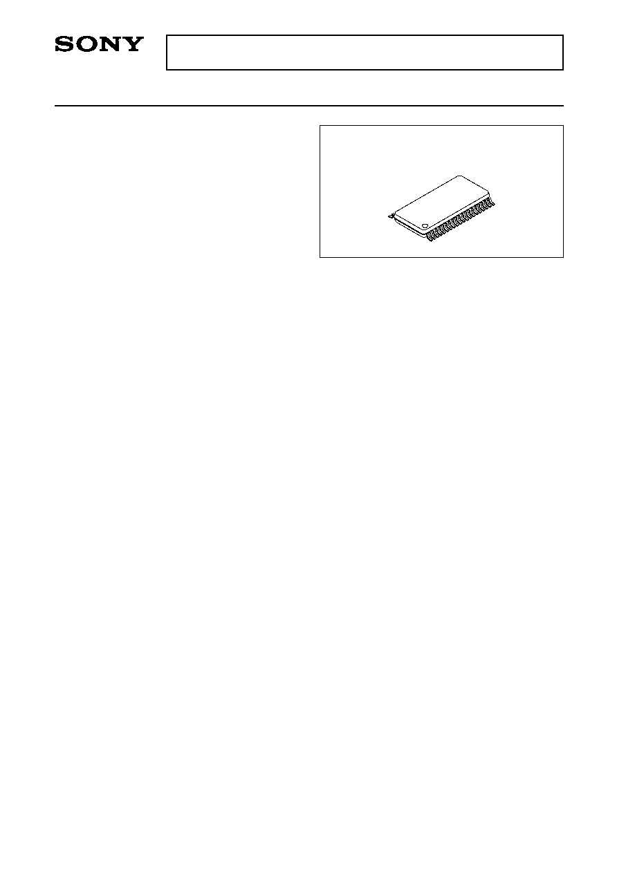
40 pin SSOP (Plastic)
E96652A82-PS
Sample-and-Hold Driver IC for LCD
Description
The CXA2504N comprises a 6-channel sample-
and-hold circuit and driver for liquid crystal display.
Features
∑ Built-in sample-and-hold circuit for phase matching
∑ Sample-and-hold circuit slew rate
280V/µs (Typ.)
∑ Driver slew rate
190V/µs (Typ.)
(for 300pF load capacitance)
∑ Sample-and-hold circuit slew rate adjustment
function
∑ Driver slew rate adjustment function
Structure
Bipolar silicon monolithic IC
Applications
∑ Liquid crystal projectors
∑ Liquid crystal viewfinders
∑ Small liquid crystal monitors
Absolute Maximum Ratings (Ta = 25∞C)
∑ Supply voltage
V
CC
1
17
V
V
CC
2
17
V
V
CC
3
7
V
∑ Input pin voltage 1
V
IN
1
1
Vcc1
V
∑ Input pin voltage 2
V
IN
2
2
Vcc3
V
∑ Digital input pin voltage VP
3
≠0.3 to Vcc3 + 0.3 V
∑ Operating temperature Topr
≠25 to +75
∞C
∑ Storage temperature
Tstg
≠55 to +150
∞C
∑ Allowable power dissipation (Ta
25∞C)
P
D
1.72
4
W
∑ Reduction rate (Ta > 25∞C)
13.8
4
mW/∞C
Operating Conditions
Supply voltage
V
CC
1
15.5 ± 0.8
V
V
CC
2
15.5 ± 0.8
V
V
CC
3
5.0 ± 0.5
V
1
Applies to Pins 4, 5, 6, 7, 8, 13, 14, 15, 16, 24,
26, 28, 34, 36 and 38.
2
Applies to Pins 17 and 39.
3
Applies to Pins 1, 2, 3, 18, 19, 20, 21 and 40.
4
When mounted on 40
◊
40mm
2
square epoxy
board.
Sony reserves the right to change products and specifications without prior notice. This information does not convey any license by
any implication or otherwise under any patents or other right. Application circuits shown, if any, are typical examples illustrating the
operation of the devices. Sony cannot assume responsibility for any problems arising out of the use of these circuits.
≠ 2 ≠
CXA2504N
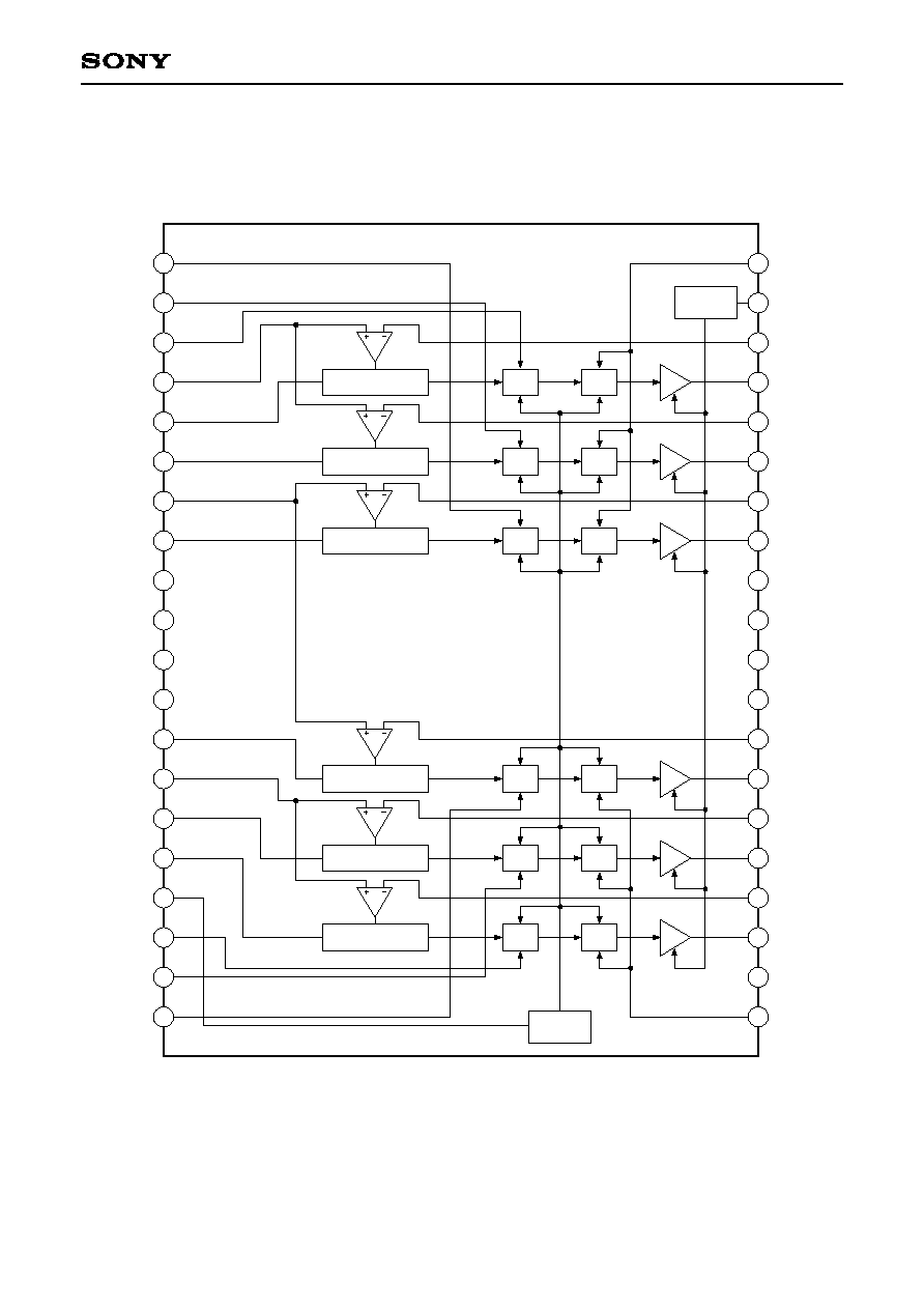
Block Diagram
Level Shifter
S/H
S/H
DR
Current
Setting
S/H
S/H
DR
S/H
S/H
DR
Level Shifter
Level Shifter
Level Shifter
S/H
S/H
DR
Level Shifter
S/H
S/H
DR
Level Shifter
S/H
S/H
DR
Current
Setting
21
22
23
24
25
26
27
28
29
30
40
39
38
37
36
35
34
31
32
33
2
3
4
5
6
7
8
9
10
11
12
13
14
15
16
17
18
19
20
1
SH4
SH5
SH6
BIAS IN56
IN6
IN5
BIAS IN34
IN4
GND
GND
GND
V
CC
1
IN3
BIAS IN12
IN2
IN1
I SH
SH1
SH2
SH3
GND
V
CC
2
SH8
BIAS OUT6
I DR
BIAS OUT5
OUT6
BIAS OUT4
OUT5
OUT4
GND
GND
SH7
V
CC
3
BIAS OUT3
BIAS OUT2
OUT3
BIAS OUT1
OUT2
OUT1
≠ 3 ≠
CXA2504N
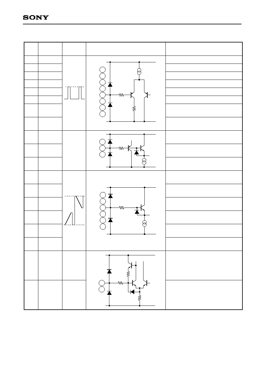
Pin Description
Pin
No.
Symbol
Pin voltage
Equivalent circuit
Description
1
2
3
18
19
20
21
40
4
7
14
5
6
8
13
15
16
17
39
SH4
SH5
SH6
SH1
SH2
SH3
SH7
SH8
BIAS IN56
BIAS IN34
BIAS IN12
IN6
IN5
IN4
IN3
IN2
IN1
I SH
I DR
CH4 sampling pulse input
CH5 sampling pulse input
CH6 sampling pulse input
CH1 sampling pulse input
CH2 sampling pulse input
CH3 sampling pulse input
Pulse input for simultaneous
resampling of CH1, 2, and 3
Pulse input for simultaneous
resampling of CH4, 5, and 6
Inputs IN5 and 6 signal center voltage
Inputs IN3 and 4 signal center voltage
Inputs IN1and 2 signal center voltage
CH6 input
1
CH5 input
1
CH4 input
1
CH3 input
1
CH2 input
1
CH1 input
1
Sets sample-and-hold circuit current.
Sample-and-hold circuit slew rate
changes.
Sets output driver circuit current.
Output driver circuit slew rate
changes.
GND
V
CC
3
21
40
2
3
18
19
20
1
100
200
200µ
V
CC
1
4
7
14
GND
200
20µ
5
6
13
15
16
V
CC
1
GND
200
100µ
8
0V
3.0 to 5.0V
2V
11.5V
V
CC
3
GND
200
10k
39
17
2k
1.2V
1.2V
1
Do not input a signal of 2V or less to IN1 to IN6.
≠ 4 ≠
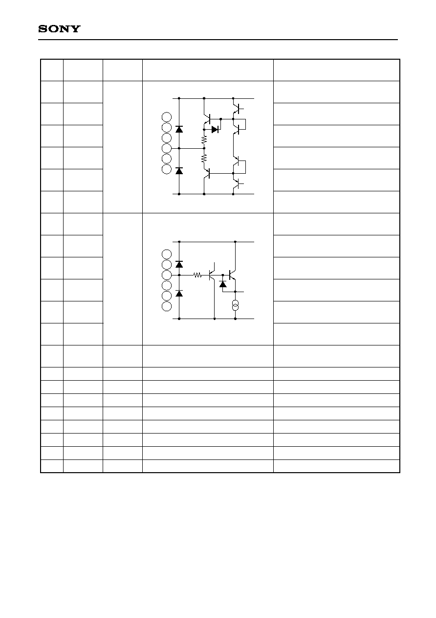
CXA2504N
Pin
No.
Symbol
Pin voltage
Equivalent circuit
Description
23
25
27
33
35
37
24
26
28
34
36
38
12
22
32
9
10
11
29
30
31
OUT1
OUT2
OUT3
OUT4
OUT5
OUT6
BIAS OUT1
BIAS OUT2
BIAS OUT3
BIAS OUT4
BIAS OUT5
BIAS OUT6
Vcc1
Vcc3
Vcc2
GND
GND
GND
GND
GND
GND
CH1 output
2
CH2 output
2
CH3 output
2
CH4 output
2
CH5 output
2
CH6 output
2
Inputs OUT1 signal center voltage
Inputs OUT2 signal center voltage
Inputs OUT3 signal center voltage
Inputs OUT4 signal center voltage
Inputs OUT5 signal center voltage
Inputs OUT6 signal center voltage
Power supply for level shifter and
S/H circuit
5V system power supply
Output driver power supply
GND
3
GND
3
GND
3
GND
3
GND
3
GND
3
GND
V
CC
2
10
10
23
25
27
37
35
33
24
26
38
36
34
V
CC
1
GND
200
20µ
28
15.5V
5.0V
15.5V
2
Power consumption varies depending on the output signal when driving load capacitance. Be careful not to
go over the package allowable power dissipation.
3
Pins 9 to 11 and 29 to 31 must be connected to GND potential; they must not be open.
≠ 5 ≠
CXA2504N
Electrical Characteristics
Unless otherwise specified:
Vcc1 = Vcc2 = 15.5V, Vcc3 = 5.0V, Ta = 25∞C
SW1
b, SW2
b, SW3
b, SW4
b, SW5
a, SW6
a, SW7
b, SW8
a, SW13
a, SW14
b,
SW15
a, SW16
a, SW18
b, SW19
b, SW20
b, SW21
b, SW24
b, SW26
b, SW28
b,
SW34
b, SW36
b, SW38
b, SW40
b
V
1
= 5V, V
2
= 5V, V
3
= 5V, V
18
= 5V, V
19
= 5V, V
20
= 5V, V
21
= 5V, V
40
= 5V, CL = 300pF
No.
1
2
3
4
5
6
7
8
9
10
11
12
13
14
15
16
17
18
19
20
21
22
23
24
25
26
27
28
29
30
31
Current consumption (1)
Current consumption (2)
Current consumption (3)
SH4 "H" pin current
SH4 "L" pin current
SH5 "H" pin current
SH5 "L" pin current
SH6 "H" pin current
SH6 "L" pin current
BIAS IN56 pin current
IN6 pin current
IN5 pin current
BIAS IN34 pin current
IN4 pin current
IN3 pin current
BIAS IN12 pin current
IN2 pin current
IN1 pin current
SH1 "H" pin current
SH1 "L" pin current
SH2 "H" pin current
SH2 "L" pin current
SH3 "H" pin current
SH3 "L" pin current
SH7 "H" pin current
SH7 "L" pin current
BIAS OUT1 pin current
BIAS OUT2 pin current
BIAS OUT3 pin current
BIAS OUT4 pin current
BIAS OUT5 pin current
SW5
b, SW6
b, SW8
b, SW13
b,
SW15
b, SW16
b,
V
1
= V
6
= V
8
= V
13
= V
15
= V
16
= 7V
SW1
b, V
1
= 5V
SW1
b, V
1
= 0V
SW2
b, V
2
= 5V
SW2
b, V
2
= 0V
SW3
b, V
3
= 5V
SW3
b, V
3
= 0V
SW4
a, V
4
= 7V
SW5
b, V
5
= 7V
SW6
b, V
6
= 7V
SW7
a, V
7
= 7V
SW8
b, V
8
= 7V
SW13
b, V
13
= 7V
SW14
a, V
14
= 7V
SW15
b, V
15
= 7V
SW16
b, V
16
= 7V
SW18
b, V
18
= 5V
SW18
b, V
18
= 0V
SW19
b, V
19
= 5V
SW19
b, V
19
= 0V
SW20
b, V
20
= 5V
SW20
b, V
20
= 0V
SW21
b, V
21
= 5V
SW21
b, V
21
= 0V
SW24
a, V
24
= 7V
SW26
a, V
26
= 7V
SW28
a, V
28
= 7V
SW34
a, V
34
= 7V
SW36
a, V
36
= 7V
--
--
--
≠0.1
≠12
≠0.1
≠12
≠0.1
≠12
≠0.2
--
--
≠0.2
--
--
≠0.2
--
--
≠0.1
≠12
≠0.1
≠12
≠0.1
≠12
≠0.1
≠12
≠0.2
≠0.2
≠0.2
≠0.2
≠0.2
17
8
12
0
≠5.0
0
≠5.0
0
≠5.0
0
0.5
0.5
0
0.5
0.5
0
0.5
0.5
0
≠5
0
≠5
0
≠5
0
≠5
0
0
0
0
0
24
14
17
0.1
--
0.1
--
0.1
--
0.2
2.0
2.0
0.2
2.0
2.0
0.2
2.0
2.0
0.1
--
0.1
--
0.1
--
0.1
--
0.2
0.2
0.2
0.2
0.2
mA
mA
mA
µA
µA
µA
µA
µA
µA
µA
µA
µA
µA
µA
µA
µA
µA
µA
µA
µA
µA
µA
µA
µA
µA
µA
µA
µA
µA
µA
µA
Item
Symbol
Min.
Typ.
Max.
Unit
Icc1
Icc2
Icc3
I
1H
I
1L
I
2H
I
2L
I
3H
I
3L
I
4
I
5
I
6
I
7
I
8
I
13
I
14
I
15
I
16
I
18H
I
18L
I
19H
I
19L
I
20H
I
20L
I
21H
I
21L
I
24
I
26
I
28
I
34
I
36
Measurement conditions
≠ 6 ≠
CXA2504N
No.
32
33
34
35
36
37
38
39
40
41
BIAS OUT6 pin current
SH8 "H" pin current
SH8 "L" pin current
I SH pin voltage
I DR pin voltage
Output potential
difference between
channels
Gain difference
between channels
Input/output gain
Sample-and-hold
slew rate (1)
Sample-and-hold
slew rate (2)
SW38
a, V
38
= 7V
SW40
b, V
40
= 5V
SW40
b, V
40
= 0V
Set SW5
b, SW6
b, SW8
b, SW13
b,
SW15
b, SW16
b,
V
5
= V
6
= V
8
= V
13
= V
15
= V
16
= 2V, 7V, 11.5V.
Measure output DC voltage for TP23, TP25, TP27,
TP33, TP35 and TP37 relative to each input DC voltage.
V
O
= MAX (output voltage ≠ input voltage)
≠
MIN (output voltage ≠ input voltage)
Set SW4
a, SW5
b, SW6
b, SW7
a,
SW8
b, SW13
b, SW14
a, SW15
b,
SW16
b, SW24
a, SW26
b, SW28
b,
SW34
b, SW36
b, SW38
b,
V
4
= V
7
= V
14
= V
24
= V
26
= V
28
= V
34
= V
36
= V
38
= 7V,
V
5
= V
6
= V
8
= V
13
= V
15
= V
16
= 2V, 11.5V.
Measure output DC voltage for TP23, TP25, TP27,
TP33, TP35 and TP37 relative to each input DC voltage.
Vdmax = MAX (output voltage (11.5V input)
≠ output voltage (2.0V input))
Vdmin = MIN (output voltage (11.5V input)
≠ output voltage (2.0V input))
And, calculate the difference between channels of its
voltage difference.
Vd =
Vdmax ≠
Vdmin
Set SW4
a, SW7
a, SW14
a, SW24
a, SW26
a,
SW28
a, SW34
a, SW36
a, SW38
a,
V
4
= V
7
= V
14
= V
24
= V
26
= V
28
= V
34
= V
36
= V
38
= 7V.
Input SG1 to (IN1) to (IN6) and measure gain between
input and output for TP23, TP25, TP27, TP33, TP35
and TP37 (refer to output waveforms (1)).
Set SW1
a, SW2
a, SW3
a, SW4
a, SW7
a,
SW14
a, SW18
a, SW19
a, SW20
a,
SW24
a, SW26
a, SW28
a, SW34
a,
SW36
a, SW38
a,
V
4
= V
7
= V
14
= V
24
= V
26
= V
28
= V
34
= V
36
= V
38
= 7V,
(SH1) to (SH6) = SG4.
Input SG2 and SG3 to (IN1) to (IN6) and measure
output waveform (2) V for TP23, TP25, TP27, TP33,
TP35 and TP37.
R
TSH1
= (V/µs)
Set SW4
a, SW7
a, SW14
a, SW21
a, SW24
a,
SW26
a, SW28
a, SW34
a, SW36
a,
SW38
a, SW40
a,
V
4
= V
7
= V
14
= V
24
= V
26
= V
28
= V
34
= V
36
= V
38
= 7V,
(SH7) = (SH8) = SG4.
Input SG2 and SG3 to (IN1) to (IN6) and measure
output waveform (2) V for TP23, TP25, TP27, TP33,
TP35 and TP37.
R
TSH2
= (V/µs)
≠0.2
≠0.1
≠12
--
--
--
--
≠0.5
220
220
0
0
≠5
1.2
1.2
--
--
≠0.1
280
280
0.2
0.1
--
--
--
25
25
--
--
--
µA
µA
µA
V
V
mV
mW
dB
V/µs
V/µs
Item
Symbol
Min.
Typ.
Max.
Unit
I
38
I
40H
I
40L
V
17
V
39
V
O
Vd
G
IO
R
TSH1
R
TSH2
Measurement conditions
V
15
◊
10≠
3
V
15
◊
10≠
3
≠ 7 ≠
CXA2504N
No.
42
43
44
45
46
47
Sample-and-hold
droop rate (1)
Sample-and-hold
droop rate (2)
Driver slew rate
SH7, SH8
output
propagation delay
time
Input
output
propagation delay
time
Input dynamic range
Set SW1
a, SW2
a, SW3
a, SW4
a, SW5
b,
SW6
b, SW7
a, SW8
b, SW13
b, SW14
a,
SW15
b, SW16
b, SW18
a, SW19
a,
SW20
a, SW24
a, SW26
a, SW28
a,
SW34
a, SW36
a, SW38
a,
V
4
= V
7
= V
14
= V
24
= V
26
= V
28
= V
34
= V
36
= V
38
= 7V,
(SH1) to (SH6) = SG5, V
5
= V
6
= V
8
= V
13
= V
15
= V
16
= 2V, 7V, 11.5V.
Measure output waveform (3) V for TP23, TP25, TP27,
TP33, TP35 and TP37 relative to each input DC.
R
D1
= (mV/µs)
Set SW4
a, SW5
b, SW6
b, SW7
a, SW8
b,
SW13
b, SW14
a, SW15
b, SW16
b,
SW21
a, SW24
a, SW26
a, SW28
a,
SW34
a, SW36
a, SW38
a, SW40
a,
V
4
= V
7
= V
14
= V
24
= V
26
= V
28
= V
34
= V
36
= V
38
= 7V,
(SH7) = (SH8) = SG5, V
5
= V
6
= V
8
= V
13
= V
15
= V
16
= 2V, 7V, 11.5V.
Measure output waveform (3) V for TP23, TP25, TP27,
TP33, TP35 and TP37 relative to each input DC.
R
D2
= (mV/µs)
Set SW4
a, SW7
a, SW14
a, SW21
a,
SW24
a, SW26
a, SW28
a, SW34
a,
SW36
a, SW38
a, SW40
a,
V
4
= V
7
= V
14
= V
24
= V
26
= V
28
= V
34
= V
36
= V
38
= 7V,
(SH7) = (SH8) = SG8.
Input SG6 and SG7 to (IN1) to (IN6) and measure
output waveform (4) t and V for TP23, TP25, TP27,
TP33, TP35 and TP37.
R
TDR
= (V/µs)
Set SW4
a, SW7
a, SW14
a, SW21
a,
SW24
a, SW26
a, SW28
a, SW34
a,
SW36
a, SW38
a, SW40
a,
V
4
= V
7
= V
14
= V
24
= V
26
= V
28
= V
34
= V
36
= V
38
= 7V,
(SH7) = (SH8) = SG8.
Input SG6 and SG7 to (IN1) to (IN6) and for each of the
four conditions for input signal rise and fall, measure
output waveform (4) t
P
for TP23, TP25, TP27, TP33,
TP35 and TP37.
Set SW4
a, SW7
a, SW14
a, SW24
a,
SW26
a, SW28
a, SW34
a, SW36
a,
SW38
a,
V
4
= V
7
= V
14
= V
24
= V
26
= V
28
= V
34
= V
36
= V
38
= 7V,
CL = 0pF.
Input SG9 and SG10 to (IN1) to (IN6) and for each of
the four conditions for input signal rise and fall,
measure output waveform (5) t
D
for TP23, TP25,
TP27, TP33, TP35 and TP37.
--
--
130
13
7
2.0
--
--
190
17
10
--
±40
±40
--
21
13
11.5
mV/
µs
mV/
µs
V/µs
ns
ns
V
Item
Symbol
Min.
Typ.
Max.
Unit
R
D1
R
D2
R
TDR
t
PLH
(H)
t
PHL
(H)
t
PLH
(L)
t
PHL
(L)
t
DLH
(H)
t
DHL
(H)
t
DLH
(L)
t
DHL
(L)
V
DIN
Measurement conditions
V
◊
0.8
t
V
10
V
10
≠ 8 ≠
CXA2504N
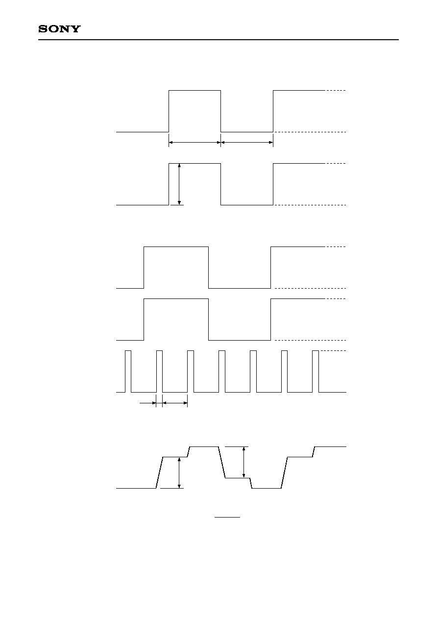
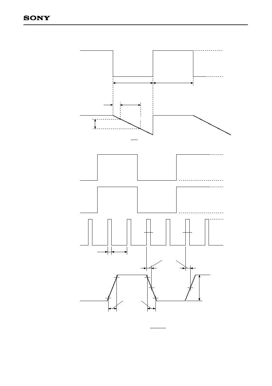
11.5V
2V
approx. 11.5V
approx. 2V
measurement
level
30µs
30µs
Input waveform SG1
Output waveform (1)
11.5V
6.5V
Input signal SG2
7V
2V
Input signal SG3
5V
0
Input signal SG4
75ns
15ns
measurement
level V
measurement
level V
Output waveform (2)
Sample-and-hold slew rate =
V
15
◊
10
≠3
SG2 and SG3 must change completely within SG4 "L" interval.
≠ 9 ≠
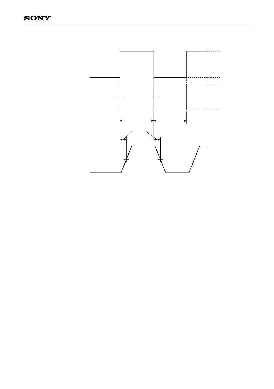
CXA2504N
5V
0V
measurement
level V
20µs
20µs
Input signal SG5
Output waveform (3)
11.5V
8V
Input signal SG6
5V
0V
Input signal SG8
75ns
15ns
10µs
droop rate =
V
10
(mV/µs)
5.5V
2V
Input signal SG7
50%
50%
measurement
level V
Output waveform (4)
Slew rate =
V
◊
0.8
t
SG5 and SG6 must change completely within SG7 "L" interval.
50%
50%
90%
10%
measurement
level t
measurement level
propagation delay
time
tp
5µs
≠ 10 ≠
CXA2504N
11.5V
8V
SG10
30µs
5.5V
2V
SG9
50%
50%
tr, tf = 1ns
tr, tf = 1ns
30µs
Output waveform (5)
50%
measurement
level
t
D
≠ 11 ≠
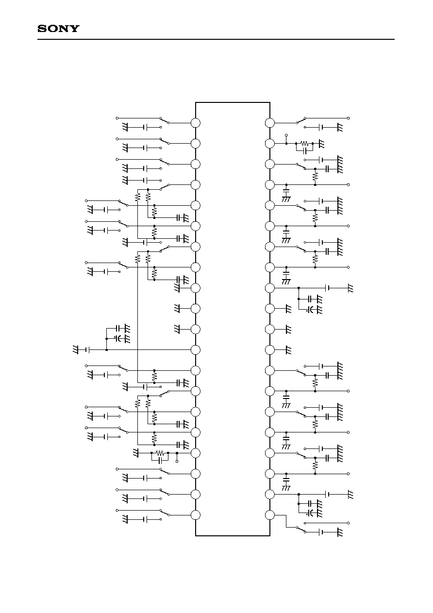
CXA2504N
(a)
(SH4)
(b)
SW1
V
1
(a)
(SH5)
(b)
SW2
V
2
(a)
(SH6)
(b)
SW3
V
3
V
4
(a)
(b)
SW4
(a)
(b)
SW5
V
5
(a)
(b)
SW6
V
6
(a)
(b)
SW7
V
7
(IN6)
(IN5)
(a)
(b)
SW8
V
8
(IN4)
V
CC
1
(a)
(b)
SW13
V
13
(IN3)
(a)
(b)
SW14
V
14
(a)
(b)
SW15
V
15
(IN2)
(a)
(b)
SW16
V
16
(IN1)
TP17
(a)
(SH1)
(b)
SW18
V
18
(a)
(SH2)
(b)
SW19
V
19
(a)
(SH3)
(b)
SW20
V
20
2
5
6
21
22
23
24
25
26
27
28
29
30
40
39
38
37
36
35
34
31
32
33
1
3
4
8
9
10
7
11
12
13
14
15
16
17
18
19
20
(a)
(SH8)
(b)
SW40
V
40
TP39
(a)
(b)
V
38
TP37
(a)
(b)
SW36
V
36
TP35
(a)
(b)
SW34
V
34
TP33
V
CC
2
SW38
(a)
(b)
V
28
TP27
SW28
(a)
(b)
V
26
TP25
SW26
(a)
(b)
V
24
TP23
SW24
V
CC
3
(a)
(SH 7)
(b)
SW21
V
21
10µ
0.1µ
CL
CL
CL
0.1µ
390k
0.1µ
390k
0.1µ
390k
0.1µ
390k
0.1µ
10µ
0.1µ
390k
0.1µ
390k
CL
CL
CL
47k
0.01µ
0.1µ
10µ
0.1µ
390k
0.1µ
390k
0.1µ
390k
390k
390k
390k
390k
390k
390k
0.1µ
390k
0.1µ
390k
0.1µ
390k
22k
0.01µ
Electrical Characteristics Measurement Circuit
≠ 12 ≠
CXA2504N
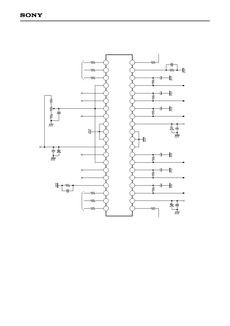
Application Circuit
0.01µ
47k
390k
1µ
1
390k
1µ
1
390k
1µ
1
390k
1µ
1
390k
1µ
1
390k
1µ
1
CH6 output
CH5 output
CH4 output
15.5V
CH3 output
CH2 output
CH1 output
5.0V
Resample-and-hold pulse input
Resample-and-hold pulse input
2
Sample-and-hold
pulse input
CH6 input
CH5 input
CH4 input
0.01µ
CH3 input
CH2 input
CH1 input
15.5V
0.01µ
22k
Sample-and-hold
pulse input
2
5
6
21
22
23
24
25
26
27
28
29
30
40
39
38
37
36
35
34
31
32
33
1
3
4
8
9
10
7
11
12
13
14
15
16
17
18
19
20
1
Use a ceramic capacitor with low leak.
2
Adjust to CH1 to 6 input signal DC voltage (within ±150mV).
Application circuits shown are typical examples illustrating the operation of the devices. Sony cannot assume responsibility for
any problems arising out of the use of these circuits or for any infringement of third party patent and other right due to same.
≠ 13 ≠
CXA2504N
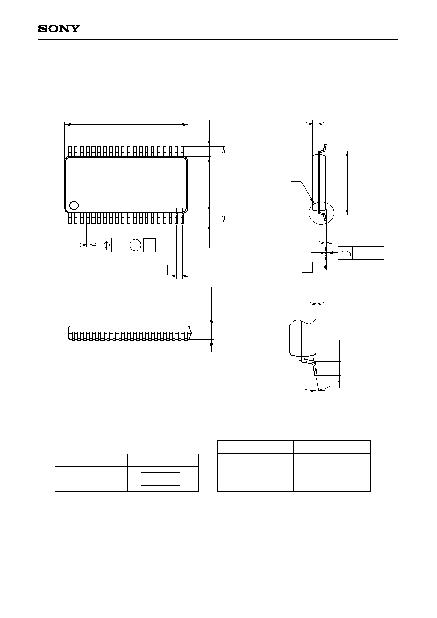
Package Outline
Unit: mm
SONY CODE
EIAJ CODE
JEDEC CODE
PACKAGE MATERIAL
LEAD TREATMENT
LEAD MATERIAL
PACKAGE WEIGHT
EPOXY RESIN
SOLDER PLATING
COPPER ALLOY
PACKAGE STRUCTURE
40PIN SSOP(PLASTIC)
8
.
4
±
0
.
4
1
.
4
5
±
0
.
2
A
13.5 ± 0.2
0.1 ± 0.1
0.3 ± 0.1
*
6
.
3
±
0
.
2
(
6
.
9
5
)
(
1
.
0
5
)
DETAIL A
0∞ to 10∞
0.65
40
21
1
20
0.3g
SSOP-40P-L111
(
1
.
0
5
)
(
1
.
0
5
)
0.15 ± 0.05
0.1
S
S
NOTE : ``*'' Dimensions do not include mold protrusion.
0.65
M
0.12
S