
©2003 Silicon Storage Technology, Inc.
S71152-05-000
9/03
1
The SST logo and SuperFlash are registered trademarks of Silicon Storage Technology, Inc.
MTP is a trademark of Silicon Storage Technology, Inc.
These specifications are subject to change without notice.
Data Sheet
256 Kbit / 512 Kbit / 1 Mbit / 2 Mbit (x8)
Many-Time Programmable Flash
SST27SF256 / SST27SF512 / SST27SF010 / SST27SF020
FEATURES:
∑
Organized as 32K x8 / 64K x8 / 128K x8 / 256K x8
∑
4.5-5.5V Read Operation
∑
Superior Reliability
≠ Endurance: At least 1000 Cycles
≠ Greater than 100 years Data Retention
∑
Low Power Consumption
≠ Active Current: 20 mA (typical)
≠ Standby Current: 10 µA (typical)
∑
Fast Read Access Time
≠ 70 ns
≠ 90 ns
∑
Fast Byte-Program Operation
≠ Byte-Program Time: 20 µs (typical)
≠ Chip Program Time:
0.7 seconds (typical) for SST27SF256
1.4 seconds (typical) for SST27SF512
2.8 seconds (typical) for SST27SF010
5.6 seconds (typical) for SST27SF020
∑
Electrical Erase Using Programmer
≠ Does not require UV source
≠ Chip-Erase Time: 100 ms (typical)
∑
TTL I/O Compatibility
∑
JEDEC Standard Byte-wide EPROM Pinouts
∑
Packages Available
≠ 32-lead PLCC
≠ 32-lead TSOP (8mm x 14mm)
≠ 28-pin PDIP for SST27SF256/512
≠ 32-pin PDIP for SST27SF010/020
PRODUCT DESCRIPTION
The SST27SF256/512/010/020 are a 32K x8 / 64K x8 /
128K x8 / 256K x8 CMOS, Many-Time Programmable
(MTP) low cost flash, manufactured with SST's proprietary,
high performance SuperFlash technology. The split-gate
cell design and thick oxide tunneling injector attain better
reliability and manufacturability compared with alternate
approaches. These MTP devices can be electrically erased
and programmed at least 1000 times using an external pro-
grammer with a 12 volt power supply. They have to be
erased prior to programming. These devices conform to
JEDEC standard pinouts for byte-wide memories.
Featuring high performance Byte-Program, the
SST27SF256/512/010/020 provide a Byte-Program time of
20 µs. Designed, manufactured, and tested for a wide
spectrum of applications, these devices are offered with an
endurance of at least 1000 cycles. Data retention is rated at
greater than 100 years.
The SST27SF256/512/010/020 are suited for applications
that require infrequent writes and low power nonvolatile
storage. These devices will improve flexibility, efficiency,
and performance while matching the low cost in nonvolatile
applications that currently use UV-EPROMs, OTPs, and
mask ROMs.
To meet surface mount and conventional through hole
requirements, the SST27SF256/512 are offered in 32-lead
PLCC, 32-lead TSOP, and 28-pin PDIP packages. The
SST27SF010/020 are offered in 32-pin PDIP, 32-lead
PLCC, and 32-lead TSOP packages. See Figures 1, 2, and
3 for pin assignments.
Device Operation
The SST27SF256/512/010/020 are a low cost flash
solution that can be used to replace existing UV-
EPROM, OTP, and mask ROM sockets. These devices
are functionally (read and program) and pin compatible
with industry standard EPROM products. In addition to
EPROM functionality, these devices also support elec-
trical Erase operation via an external programmer. They
do not require a UV source to erase, and therefore the
packages do not have a window.
Read
The Read operation of the SST27SF256/512/010/020 is
controlled by CE# and OE#. Both CE# and OE# have to be
low for the system to obtain data from the outputs. Once
the address is stable, the address access time is equal to
the delay from CE# to output (T
CE
). Data is available at the
output after a delay of T
OE
from the falling edge of OE#,
assuming that CE# pin has been low and the addresses
have been stable for at least T
CE
-T
OE.
When the CE# pin is
high, the chip is deselected and a typical standby current of
10 µA is consumed. OE# is the output control and is used
to gate data from the output pins. The data bus is in high
impedance state when either CE# or OE# is high.
SST27SF256 / 512 / 010 / 0205.0V-Read 256Kb / 512Kb / 1Mb / 2Mb (x8) MTP flash memories
2
Data Sheet
256 Kbit / 512 Kbit / 1 Mbit / 2 Mbit Many-Time Programmable Flash
SST27SF256 / SST27SF512 / SST27SF010 / SST27SF020
©2003 Silicon Storage Technology, Inc.
S71152-05-000
9/03
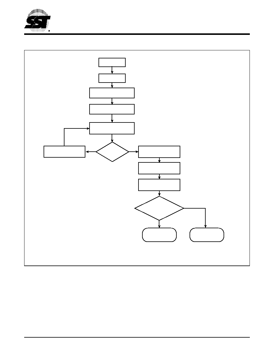
Byte-Program Operation
The SST27SF256/512/010/020 are programmed by using
an external programmer. The programming mode for
SST27SF256/010/020 is activated by asserting 11.4-12.6V
on V
PP
pin, V
DD
= 4.5-5.5V, V
IL
on CE# pin, and
V
IH
on
OE# pin. The programming mode for SST27SF512 is acti-
vated by asserting 11.4-12.6V on OE#/V
PP
pin, V
DD
= 4.5-
5.5V, and V
IL
on CE# pin. These devices are programmed
byte-by-byte with the desired data at the desired address
using a single pulse (CE# pin low for SST27SF256/512
and PGM# pin low for SST27SF010/020) of 20 µs. Using
the MTP programming algorithm, the Byte-Programming
process continues byte-by-byte until the entire chip has
been programmed.
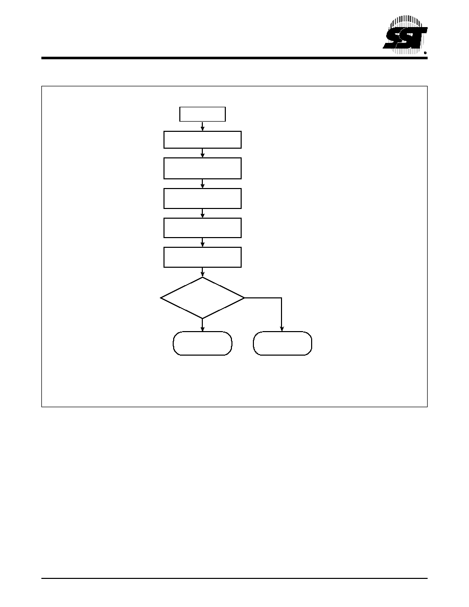
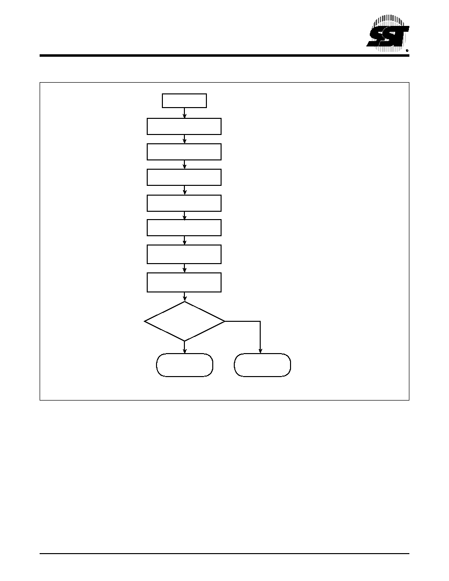
Chip-Erase Operation
The only way to change a data from a "0" to "1" is by electri-
cal erase that changes every bit in the device to "1". Unlike
traditional EPROMs, which use UV light to do the Chip-
Erase, the SST27SF256/512/010/020 uses an electrical
Chip-Erase operation. This saves a significant amount of
time (about 30 minutes for each Erase operation). The
entire chip can be erased in a single pulse of 100 ms (CE#
pin low for SST27SF256/512 and PGM# pin for
SST27SF010/020). In order to activate the Erase mode for
SST27SF256/010/020, the 11.4-12.6V is applied to V
PP
and A
9
pins, V
DD
= 4.5-5.5V, V
IL
on CE# pin, and
V
IH
on
OE# pin. In order to activate Erase mode for SST27SF512,
the 11.4-12.6V is applied to OE#/V
PP
and A
9
pins, V
DD
=
4.5-5.5V, and V
IL
on CE# pin. All other address and data
pins are "don't care". The falling edge of CE# (PGM# for
SST27SF010/020) will start the Chip-Erase operation.
Once the chip has been erased, all bytes must be verified
for FFH. Refer to Figures 13, 14, and 15 for the flowcharts.
Product Identification Mode
The Product Identification mode identifies the devices as
the SST27SF256, SST27SF512, SST27SF010 and
SST27SF020 and manufacturer as SST. This mode may
be accessed by the hardware method. To activate this
mode for SST27SF256/010/020, the programming equip-
ment must force V
H
(11.4-12.6V) on address A
9
with V
PP
pin at V
DD
(4.5-5.5V) or V
SS
. To activate this mode for
SST27SF512, the programming equipment must force V
H
(11.4-12.6V) on address A
9
with OE#/V
PP
pin at V
IL
. Two
identifier bytes may then be sequenced from the device
outputs by toggling address line A
0
. For details, see Tables
3, 4, and 5 for hardware operation.
TABLE
1: P
RODUCT
I
DENTIFICATION
Address
Data
Manufacturer's ID
0000H
BFH
Device ID
SST27SF256
0001H
A3H
SST27SF512
0001H
A4H
SST27SF010
0001H
A5H
SST27SF020
0001H
A6H
T1.1 1152
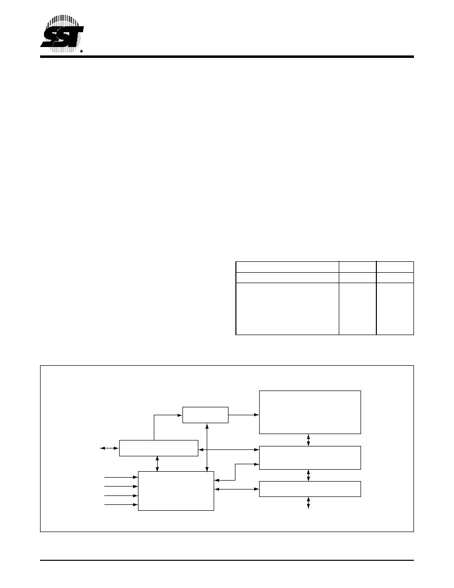
Y-Decoder
I/O Buffers
1152 B1.1
Address Buffer
X-Decoder
DQ7 - DQ0
A14 - A0
A9
OE#
CE#
VPP
SuperFlash
Memory
Control Logic
F
UNCTIONAL
B
LOCK
D
IAGRAM
OF
THE
SST27SF256
Data Sheet
256 Kbit / 512 Kbit / 1 Mbit / 2 Mbit Many-Time Programmable Flash
SST27SF256 / SST27SF512 / SST27SF010 / SST27SF020
3
©2003 Silicon Storage Technology, Inc.
S71152-05-000
9/03
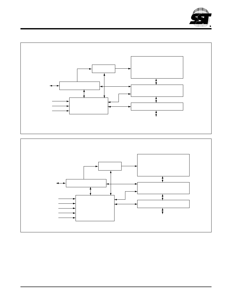
Y-Decoder
I/O Buffers
1152 B2.1
Address Buffer
X-Decoder
DQ7 - DQ0
A15 - A0
A9
OE#/VPP
CE#
SuperFlash
Memory
Control Logic
F
UNCTIONAL
B
LOCK
D
IAGRAM
OF
THE
SST27SF512
Y-Decoder
I/O Buffers
1152 B3.2
Address Buffer
X-Decoder
DQ7 - DQ0
AMS - A0
A9
OE#
CE#
SuperFlash
Memory
Control Logic
PGM#
VPP
AMS = A17 for SST27SF020, A16 for SST27SF010
F
UNCTIONAL
B
LOCK
D
IAGRAM
OF
THE
SST27SF010/020
4
Data Sheet
256 Kbit / 512 Kbit / 1 Mbit / 2 Mbit Many-Time Programmable Flash
SST27SF256 / SST27SF512 / SST27SF010 / SST27SF020
©2003 Silicon Storage Technology, Inc.
S71152-05-000
9/03
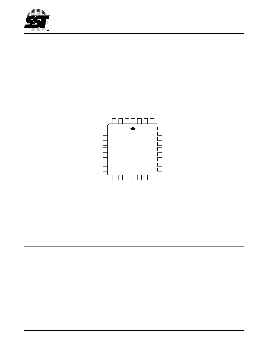
FIGURE 1: P
IN
A
SSIGNMENTS
FOR
32-
LEAD
PLCC
1152 32-plcc P1.3
SST27SF256
SST27SF512
SST27SF512
SST27SF010
SST27SF010
SST27SF020
SST27SF020
SST27SF256
SST27SF256
SST27SF512
SST27SF512
SST27SF010
SST27SF010
SST27SF020
SST27SF020
SST27SF256
5
6
7
8
9
10
11
12
13
29
28
27
26
25
24
23
22
21
A6
A5
A4
A3
A2
A1
A0
NC
DQ0
A6
A5
A4
A3
A2
A1
A0
NC
DQ0
A7
A6
A5
A4
A3
A2
A1
A0
DQ0
A7
A6
A5
A4
A3
A2
A1
A0
DQ0
A8
A9
A11
NC
OE#
A10
CE#
DQ7
DQ6
A8
A9
A11
NC
OE#/VPP
A10
CE#
DQ7
DQ6
A14
A13
A8
A9
A11
OE#
A10
CE#
DQ7
A14
A13
A8
A9
A11
OE#
A10
CE#
DQ7
4 3 2 1 32 31 30
A7
A12
V
PP
NC
V
DD
A14
A13
A7
A12
A15
NC
V
DD
A14
A13
A12
A15
A16
V
PP
V
DD
PGM#
NC
A12
A15
A16
V
PP
V
DD
PGM#
A17
32-lead PLCC
Top View
14 15 16 17 18 19 20
DQ1
DQ2
V
SS
NC
DQ3
DQ4
DQ5
DQ1
DQ2
V
SS
NC
DQ3
DQ4
DQ5
DQ1
DQ2
V
SS
DQ3
DQ4
DQ5
DQ6
DQ1
DQ2
V
SS
DQ3
DQ4
DQ5
DQ6
Data Sheet
256 Kbit / 512 Kbit / 1 Mbit / 2 Mbit Many-Time Programmable Flash
SST27SF256 / SST27SF512 / SST27SF010 / SST27SF020
5
©2003 Silicon Storage Technology, Inc.
S71152-05-000
9/03
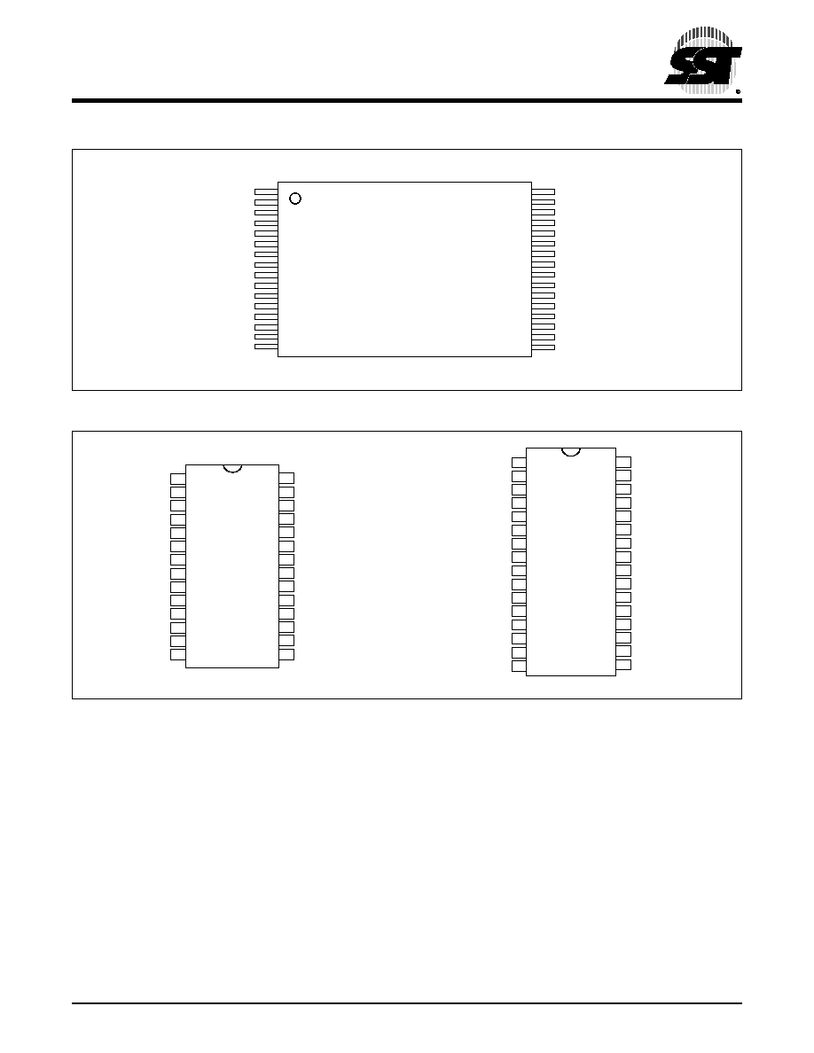
FIGURE 2: P
IN
A
SSIGNMENTS
FOR
32-
LEAD
TSOP (8
MM
X
14
MM
)
FIGURE 3: P
IN
A
SSIGNMENTS
FOR
28-
PIN
AND
32-
PIN
PDIP
1152 32-tsop P2.1
A11
A9
A8
A13
A14
NC
NC
VDD
VPP
NC
NC
A12
A7
A6
A5
A4
A11
A9
A8
A13
A14
NC
NC
VDD
NC
NC
A15
A12
A7
A6
A5
A4
A11
A9
A8
A13
A14
NC
PGM#
VDD
VPP
A16
A15
A12
A7
A6
A5
A4
A11
A9
A8
A13
A14
A17
PGM#
VDD
VPP
A16
A15
A12
A7
A6
A5
A4
1
2
3
4
5
6
7
8
9
10
11
12
13
14
15
16
OE#
A10
CE#
DQ7
DQ6
DQ5
DQ4
DQ3
VSS
DQ2
DQ1
DQ0
A0
A1
A2
A3
OE#/VPP
A10
CE#
DQ7
DQ6
DQ5
DQ4
DQ3
VSS
DQ2
DQ1
DQ0
A0
A1
A2
A3
OE#
A10
CE#
DQ7
DQ6
DQ5
DQ4
DQ3
VSS
DQ2
DQ1
DQ0
A0
A1
A2
A3
OE#
A10
CE#
DQ7
DQ6
DQ5
DQ4
DQ3
VSS
DQ2
DQ1
DQ0
A0
A1
A2
A3
32
31
30
29
28
27
26
25
24
23
22
21
20
19
18
17
Standard Pinout
Top View
Die Up
SST27SF256
SST27SF512
SST27SF512
SST27SF010
SST27SF010
SST27SF020
SST27SF020
SST27SF256
1
2
3
4
5
6
7
8
9
10
11
12
13
14
15
16
32-pin
PDIP
Top View
VPP
A16
A15
A12
A7
A6
A5
A4
A3
A2
A1
A0
DQ0
DQ1
DQ2
VSS
VPP
A16
A15
A12
A7
A6
A5
A4
A3
A2
A1
A0
DQ0
DQ1
DQ2
VSS
32
31
30
29
28
27
26
25
24
23
22
21
20
19
18
17
VDD
PGM#
NC
A14
A13
A8
A9
A11
OE#
A10
CE#
DQ7
DQ6
DQ5
DQ4
DQ3
VDD
PGM#
A17
A14
A13
A8
A9
A11
OE#
A10
CE#
DQ7
DQ6
DQ5
DQ4
DQ3
1152 32-pdip P4.1
SST27SF010
SST27SF010
SST27SF020
SST27SF020
1
2
3
4
5
6
7
8
9
10
11
12
13
14
28-pin
PDIP
Top View
VPP
A12
A7
A6
A5
A4
A3
A2
A1
A0
DQ0
DQ1
DQ2
VSS
A15
A12
A7
A6
A5
A4
A3
A2
A1
A0
DQ0
DQ1
DQ2
VSS
28
27
26
25
24
23
22
21
20
19
18
17
16
15
VDD
A14
A13
A8
A9
A11
OE#
A10
CE#
DQ7
DQ6
DQ5
DQ4
DQ3
VDD
A14
A13
A8
A9
A11
OE#/VPP
A10
CE#
DQ7
DQ6
DQ5
DQ4
DQ3
1152 28-pdip P3.1
SST27SF512
SST27SF256
SST27SF512
SST27SF256
6
Data Sheet
256 Kbit / 512 Kbit / 1 Mbit / 2 Mbit Many-Time Programmable Flash
SST27SF256 / SST27SF512 / SST27SF010 / SST27SF020
©2003 Silicon Storage Technology, Inc.
S71152-05-000
9/03
Note: V
PPH
= 11.4-12.6V, V
H
= 11.4-12.6V
Note: V
PPH
= 11.4-12.6V, V
H
= 11.4-12.6V
TABLE
2: P
IN
D
ESCRIPTION
Symbol
Pin Name
Functions
A
MS
1
-A
0
Address Inputs
To provide memory addresses
DQ
7
-DQ
0
Data Input/output
To output data during Read cycles and receive input data during Program cycles
The outputs are in tri-state when OE# or CE# is high.
CE#
Chip Enable
To activate the device when CE# is low
OE#
Output Enable
For SST27SF256/010/020, to gate the data output buffers during Read operation
OE#/V
PP
Output Enable/V
PP
For SST27SF512, to gate the data output buffers during Read operation and high voltage
pin during Chip-Erase and programming operation
V
PP
Power Supply for
Program or Erase
For SST27SF256/010/020, high voltage pin during Chip-Erase and programming opera-
tion 11.4-12.6V
V
DD
Power Supply
To provide 5.0V supply (4.5-5.5V)
V
SS
Ground
NC
No Connection
Unconnected pins.
T2.4 1152
1. A
MS
= Most significant address
A
MS
= A
14
for SST27SF256, A
15
for SST27SF512, A
16
for SST27SF010, and A
17
for SST27SF020
TABLE
3: O
PERATION
M
ODES
S
ELECTION
FOR
SST27SF256
Mode
CE#
OE#
V
PP
A
9
DQ
Address
Read
V
IL
V
IL
V
DD
or V
SS
A
IN
D
OUT
A
IN
Output Disable
V
IL
V
IH
V
DD
or V
SS
X
1
1. X can be V
IL
or V
IH,
but no other value.
High Z
X
Byte-Program
V
IL
V
IH
V
PPH
A
IN
D
IN
A
IN
Standby
V
IH
X
V
DD
or V
SS
X
High Z
X
Chip-Erase
V
IL
V
IH
V
PPH
V
H
High Z
X
Program/Erase Inhibit
V
IH
X
V
PPH
X
High Z
X
Product Identification
V
IL
V
IL
V
DD
or V
SS
V
H
Manufacturer's ID (BFH)
Device ID (A3H)
A
14
-A
1
=V
IL
, A
0
=V
IL
A
14
-A
1
=V
IL
, A
0
=V
IH
T3.2 1152
TABLE
4: O
PERATION
M
ODES
S
ELECTION
FOR
SST27SF512
Mode
CE#
OE#/V
PP
A
9
DQ
Address
Read
V
IL
V
IL
A
IN
D
OUT
A
IN
Output Disable
V
IL
V
IH
X
1
1. X can be V
IL
or V
IH,
but no other value.
High Z
X
Program
V
IL
V
PPH
A
IN
D
IN
A
IN
Standby
V
IH
X
X
High Z
X
Chip-Erase
V
IL
V
PPH
V
H
High Z
X
Program/Erase Inhibit
V
IH
V
PPH
X
High Z
X
Product Identification
V
IL
V
IL
V
H
Manufacturer's ID (BFH)
Device ID (A4H)
A
15
-A
1
=V
IL
, A
0
=V
IL
A
15
-A
1
=V
IL
, A
0
=V
IH
T4.2 1152
Data Sheet
256 Kbit / 512 Kbit / 1 Mbit / 2 Mbit Many-Time Programmable Flash
SST27SF256 / SST27SF512 / SST27SF010 / SST27SF020
7
©2003 Silicon Storage Technology, Inc.
S71152-05-000
9/03
Note: V
PPH
= 11.4-12.6V, V
H
= 11.4-12.6V
TABLE
5: O
PERATION
M
ODES
S
ELECTION
FOR
SST27SF010/020
Mode
CE#
OE#
PGM#
A
9
V
PP
DQ
Address
Read
V
IL
V
IL
X
1
A
IN
V
DD
or V
SS
D
OUT
A
IN
Output Disable
V
IL
V
IH
X
X
V
DD
or V
SS
High Z
A
IN
Program
V
IL
V
IH
V
IL
A
IN
V
PPH
D
IN
A
IN
Standby
V
IH
X
X
X
V
DD
or V
SS
High Z
X
Chip-Erase
V
IL
V
IH
V
IL
V
H
V
PPH
High Z
X
Program/Erase Inhibit
V
IH
X
X
X
V
PPH
High Z
X
Product Identification
V
IL
V
IL
X
V
H
V
DD
or V
SS
Manufacturer's ID (BFH)
Device ID
2
A
MS
3
- A
1
=V
IL
, A
0
=V
IL
A
MS
3
- A
1
=V
IL
, A
0
=V
IH
T5.2 1152
1. X can be V
IL
or V
IH,
but no other value.
2. Device ID = A5H for SST27SF010 and A6H for SST27SF020
3. A
MS
= Most significant address
A
MS
= A
16
for SST27SF010 and A
17
for SST27SF020
Absolute Maximum Stress Ratings (Applied conditions greater than those listed under "Absolute Maximum
Stress Ratings" may cause permanent damage to the device. This is a stress rating only and functional operation
of the device at these conditions or conditions greater than those defined in the operational sections of this data
sheet is not implied. Exposure to absolute maximum stress rating conditions may affect device reliability.)
Temperature Under Bias . . . . . . . . . . . . . . . . . . . . . . . . . . . . . . . . . . . . . . . . . . . . . . . . . . . . . . . . . -55∞C to +125∞C
Storage Temperature . . . . . . . . . . . . . . . . . . . . . . . . . . . . . . . . . . . . . . . . . . . . . . . . . . . . . . . . . . . -65∞C to +150∞C
D. C. Voltage on Any Pin to Ground Potential . . . . . . . . . . . . . . . . . . . . . . . . . . . . . . . . . . . . . . . . -0.5V to V
DD
+0.5V
Transient Voltage (<20 ns) on Any Pin to Ground Potential . . . . . . . . . . . . . . . . . . . . . . . . . . . . . -2.0V to V
DD
+2.0V
Voltage on A
9
and V
PP
Pin to Ground Potential . . . . . . . . . . . . . . . . . . . . . . . . . . . . . . . . . . . . . . . . . -0.5V to 14.0V
Package Power Dissipation Capability (Ta = 25∞C) . . . . . . . . . . . . . . . . . . . . . . . . . . . . . . . . . . . . . . . . . . . . . . 1.0W
Through Hold Lead Soldering Temperature (10 Seconds) . . . . . . . . . . . . . . . . . . . . . . . . . . . . . . . . . . . . . . . 300∞C
Surface Mount Lead Soldering Temperature (3 Seconds) . . . . . . . . . . . . . . . . . . . . . . . . . . . . . . . . . . . . . . . 240∞C
Output Short Circuit Current
1
. . . . . . . . . . . . . . . . . . . . . . . . . . . . . . . . . . . . . . . . . . . . . . . . . . . . . . . . . . . . 100 mA
1. Outputs shorted for no more than one second. No more than one output shorted at a time.
O
PERATING
R
ANGE
Range
Ambient Temp
V
DD
V
PP
Commercial
0∞C to +70∞C
4.5-5.5V
11.4-12.6V
AC C
ONDITIONS
OF
T
EST
Input Rise/Fall Time . . . . . . . . . . . 10 ns
Output Load . . . . . . . . . . . . . . . . . C
L
= 100 pF for 90 ns
Output Load . . . . . . . . . . . . . . . . . C
L
= 30 pF for 70 ns
See Figures 11 and 12

8
Data Sheet
256 Kbit / 512 Kbit / 1 Mbit / 2 Mbit Many-Time Programmable Flash
SST27SF256 / SST27SF512 / SST27SF010 / SST27SF020
©2003 Silicon Storage Technology, Inc.
S71152-05-000
9/03
TABLE
6: R
EAD
M
ODE
DC O
PERATING
C
HARACTERISTICS
FOR
SST27SF256/512/010/020
V
DD
= 4.5-5.5V, V
PP
=V
DD
OR
V
SS (Ta = 0∞C to +70∞C (Commercial))
Symbol Parameter
Limits
Test Conditions
Min
Max
Units
I
DD
V
DD
Read Current
Address input=V
ILT
/V
IHT
at f=1/T
RC
Min
V
DD
=V
DD
Max
30
mA
CE#=OE#=V
IL
, all I/Os open
I
PPR
V
PP
Read Current
Address input=V
ILT
/V
IHT
at f=1/T
RC
Min
V
DD
=V
DD
Max, V
PP
=V
DD
100
µA
CE#=OE#=V
IL
, all I/Os open
I
SB1
Standby V
DD
Current
(TTL input)
3
mA
CE#=V
IH
, V
DD
=V
DD
Max
I
SB2
Standby V
DD
Current
(CMOS input)
100
µA
CE#=V
DD
-0.3
V
DD
=V
DD
Max
I
LI
Input Leakage Current
1
µA
V
IN
=GND to V
DD
, V
DD
=V
DD
Max
I
LO
Output Leakage Current
10
µA
V
OUT
=GND to V
DD
, V
DD
=V
DD
Max
V
IL
Input Low Voltage
0.8
V
V
DD
=V
DD
Min
V
IH
Input High Voltage
2.0
V
DD
+0.5
V
V
DD
=V
DD
Max
V
OL
Output Low Voltage
0.2
V
I
OL
=2.1 mA, V
DD
=V
DD
Min
V
OH
Output High Voltage
2.4
V
I
OH
=-400 µA, V
DD
=V
DD
Min
I
H
Supervoltage Current for A
9
200
µA
CE#=OE#=V
IL
, A
9
=V
H
Max
T6.6 1152
TABLE
7: P
ROGRAM
/E
RASE
DC O
PERATING
C
HARACTERISTICS
FOR
SST27SF256
V
DD
=4.5-5.5V, V
PP
=V
PPH (Ta=25∞C±5∞C)
Symbol Parameter
Limits
Test Conditions
Min
Max
Units
I
DD
V
DD
Erase or Program Current
30
mA
CE#=V
IL,
OE#=V
IH
, V
PP
=11.4-12.6V, V
DD
=V
DD
Max
I
PP
V
PP
Erase or Program Current
1
mA
CE#=V
IL,
OE#=V
IH
, V
PP
=11.4-12.6V, V
DD
=V
DD
Max
I
LI
Input Leakage Current
1
µA
V
IN
=GND to V
DD
, V
DD
=V
DD
Max
I
LO
Output Leakage Current
10
µA
V
OUT
=GND to V
DD
, V
DD
=V
DD
Max
V
H
Supervoltage for A
9
11.4
12.6
V
CE#=OE#=V
IL,
I
H
Supervoltage Current for A
9
200
µA
CE#=OE#=V
IL,
A
9
=V
H
Max
V
PPH
High Voltage for V
PP
Pin
11.4
12.6
V
T7.4 1152
Data Sheet
256 Kbit / 512 Kbit / 1 Mbit / 2 Mbit Many-Time Programmable Flash
SST27SF256 / SST27SF512 / SST27SF010 / SST27SF020
9
©2003 Silicon Storage Technology, Inc.
S71152-05-000
9/03
TABLE
8: P
ROGRAM
/E
RASE
DC O
PERATING
C
HARACTERISTICS
FOR
SST27SF512
V
DD
=4.5-5.5V, V
PP
=V
PPH (Ta=25∞C±5∞C)
Symbol Parameter
Limits
Test Conditions
Min
Max
Units
I
DD
V
DD
Erase or Program Current
30
mA
CE#=V
IL,
OE#/V
PP
=11.4-12.6V, V
DD
=V
DD
Max
I
PP
V
PP
Erase or Program Current
1
mA
CE#=V
IL,
OE#/V
PP
=11.4-12.6V, V
DD
=V
DD
Max
I
LI
Input Leakage Current
1
µA
V
IN
=GND to V
DD
, V
DD
=V
DD
Max
I
LO
Output Leakage Current
10
µA
V
OUT
=GND to V
DD
, V
DD
=V
DD
Max
V
H
Supervoltage for A
9
11.4
12.6
V
CE#=OE#/V
PP
=V
IL,
I
H
Supervoltage Current for A
9
200
µA
CE#=OE#/V
PP
=V
IL,
A
9
=V
H
Max
V
PPH
High Voltage for OE#/V
PP
Pin
11.4
12.6
V
T8.4 1152
TABLE
9: P
ROGRAM
/E
RASE
DC O
PERATING
C
HARACTERISTICS
FOR
SST27SF010/020
V
DD
=4.5-5.5V, V
PP
=V
PPH (Ta=25∞C±5∞C)
Symbol Parameter
Limits
Test Conditions
Min
Max
Units
I
DD
V
DD
Erase or Program Current
30
mA
CE#=PGM#=V
IL,
OE#=V
IH
, V
PP
=11.4-12.6V,
V
DD
=V
DD
Max
I
PP
V
PP
Erase or Program Current
1
mA
CE#=PGM#=V
IL,
OE#=V
IH
, V
PP
=11.4-12.6V,
V
DD
=V
DD
Max
I
LI
Input Leakage Current
1
µA
V
IN
=GND to V
DD
, V
DD
=V
DD
Max
I
LO
Output Leakage Current
10
µA
V
OUT
=GND to V
DD
, V
DD
=V
DD
Max
V
H
Supervoltage for A
9
11.4
12.6
V
CE#=OE#=V
IL,
I
H
Supervoltage Current for A
9
200
µA
CE#=OE#=V
IL,
A
9
=V
H
Max
V
PPH
High Voltage for V
PP
Pin
11.4
12.6
V
T9.4 1152
TABLE 10: R
ECOMMENDED
S
YSTEM
P
OWER
-
UP
T
IMINGS
Symbol
Parameter
Minimum
Units
T
PU-READ
1
1. This parameter is measured only for initial qualification and after a design or process change that could affect this parameter.
Power-up to Read Operation
100
µs
T
PU-WRITE
1
Power-up to Write Operation
100
µs
T10.1 1152
TABLE 11: C
APACITANCE
(Ta = 25∞C, f=1 Mhz, other pins open)
Parameter
Description
Test Condition
Maximum
C
I/O
1
1. This parameter is measured only for initial qualification and after a design or process change that could affect this parameter.
I/O Pin Capacitance
V
I/O
= 0V
12 pF
C
IN
1
Input Capacitance
V
IN
= 0V
6 pF
T11.0 1152

10
Data Sheet
256 Kbit / 512 Kbit / 1 Mbit / 2 Mbit Many-Time Programmable Flash
SST27SF256 / SST27SF512 / SST27SF010 / SST27SF020
©2003 Silicon Storage Technology, Inc.
S71152-05-000
9/03
AC CHARACTERISTICS
TABLE 12: R
ELIABILITY
C
HARACTERISTICS
Symbol
Parameter
Minimum Specification
Units
Test Method
N
END
1
Endurance
1000
Cycles
JEDEC Standard A117
T
DR
1
Data Retention
100
Years
JEDEC Standard A103
I
LTH
1
Latch Up
100
mA
JEDEC Standard 78
T12.2 1152
1. This parameter is measured only for initial qualification and after a design or process change that could affect this parameter.
TABLE 13: R
EAD
C
YCLE
T
IMING
P
ARAMETERS
V
DD
= 4.5-5.5V
(Ta = 0∞C to +70∞C (Commercial))
Symbol
Parameter
SST27SF256-70
SST27SF512-70
SST27SF010-70
SST27SF020-70
SST27SF256-90
SST27SF512-90
SST27SF010-90
SST27SF020-90
Units
Min
Max
Min
Max
T
RC
Read Cycle Time
70
90
ns
T
CE
Chip Enable Access Time
70
90
ns
T
AA
Address Access Time
70
90
ns
T
OE
Output Enable Access Time
35
45
ns
T
CLZ
1
1. This parameter is measured only for initial qualification and after a design or process change that could affect this parameter.
CE# Low to Active Output
0
0
ns
T
OLZ
1
OE# Low to Active Output
0
0
ns
T
CHZ
1
CE# High to High-Z Output
25
30
ns
T
OHZ
1
OE# High to High-Z Output
25
30
ns
T
OH
1
Output Hold from Address Change
0
0
ns
T13.2 1152
TABLE 14: P
ROGRAM
/E
RASE
C
YCLE
T
IMING
P
ARAMETERS
FOR
SST27SF256
Symbol
Parameter
Min
Max
Units
T
AS
Address Setup Time
1
µs
T
AH
Address Hold Time
1
µs
T
PRT
V
PP
Pulse Rise Time
50
ns
T
VPS
V
PP
Setup Time
1
µs
T
VPH
V
PP
Hold Time
1
µs
T
PW
CE# Program Pulse Width
20
30
µs
T
EW
CE# Erase Pulse Width
100
500
ms
T
DS
Data Setup Time
1
µs
T
DH
Data Hold Time
1
µs
T
VR
V
PP
and A
9
Recovery Time
1
µs
T
ART
A
9
Rise Time to 12V during Erase
50
ns
T
A9S
A
9
Setup Time during Erase
1
µs
T
A9H
A
9
Hold Time during Erase
1
µs
T14.0 1152
Data Sheet
256 Kbit / 512 Kbit / 1 Mbit / 2 Mbit Many-Time Programmable Flash
SST27SF256 / SST27SF512 / SST27SF010 / SST27SF020
11
©2003 Silicon Storage Technology, Inc.
S71152-05-000
9/03
TABLE 15: P
ROGRAM
/E
RASE
C
YCLE
T
IMING
P
ARAMETERS
FOR
SST27SF512
Symbol
Parameter
Min
Max
Units
T
AS
Address Setup Time
1
µs
T
AH
Address Hold Time
1
µs
T
PRT
OE#/V
PP
Pulse Rise Time
50
ns
T
VPS
OE#/V
PP
Setup Time
1
µs
T
VPH
OE#/V
PP
Hold Time
1
µs
T
PW
CE# Program Pulse Width
20
30
µs
T
EW
CE# Erase Pulse Width
100
500
ms
T
DS
Data Setup Time
1
µs
T
DH
Data Hold Time
1
µs
T
VR
OE#/V
PP
and A
9
Recovery Time
1
µs
T
ART
A
9
Rise Time to 12V during Erase
50
ns
T
A9S
A
9
Setup Time during Erase
1
µs
T
A9H
A
9
Hold Time during Erase
1
µs
T15.0 1152
TABLE 16: P
ROGRAM
/E
RASE
C
YCLE
T
IMING
P
ARAMETERS
FOR
SST27SF010/020
Symbol
Parameter
Min
Max
Units
T
CES
CE# Setup Time
1
µs
T
CEH
CE# Hold Time
1
µs
T
AS
Address Setup Time
1
µs
T
AH
Address Hold Time
1
µs
T
PRT
V
PP
Pulse Rise Time
50
ns
T
VPS
V
PP
Setup Time
1
µs
T
VPH
V
PP
Hold Time
1
µs
T
PW
PGM# Program Pulse Width
20
30
µs
T
EW
PGM# Erase Pulse Width
100
500
ms
T
DS
Data Setup Time
1
µs
T
DH
Data Hold Time
1
µs
T
VR
A
9
Recovery Time for Erase
1
µs
T
ART
A
9
Rise Time to 12V during Erase
50
ns
T
A9S
A
9
Setup Time during Erase
1
µs
T
A9H
A
9
Hold Time during Erase
1
µs
T16.0 1152
12
Data Sheet
256 Kbit / 512 Kbit / 1 Mbit / 2 Mbit Many-Time Programmable Flash
SST27SF256 / SST27SF512 / SST27SF010 / SST27SF020
©2003 Silicon Storage Technology, Inc.
S71152-05-000
9/03
FIGURE 4: R
EAD
C
YCLE
T
IMING
D
IAGRAM
FOR
SST27SF256/512/010/020
FIGURE 5: C
HIP
-E
RASE
T
IMING
D
IAGRAM
FOR
SST27SF256
1152 F03.0
DATA VALID
DATA VALID
TCLZ
TOLZ
TOH
TRC
TAA
TOE
TOHZ
TCHZ
HIGH-Z
DQ7-0
OE#
CE#
ADDRESS
TCE
1152 F04a.1
TA9H
TVR
TVPH
TVPS
TEW
TPRT
VDD
VSS
VPP
A9
VPPH
VPPH
VIH
VIH
VIL
DQ7-0
CE#
OE#
ADDRESS
(EXCEPT A9)
TA9S
TART
TVR
Data Sheet
256 Kbit / 512 Kbit / 1 Mbit / 2 Mbit Many-Time Programmable Flash
SST27SF256 / SST27SF512 / SST27SF010 / SST27SF020
13
©2003 Silicon Storage Technology, Inc.
S71152-05-000
9/03
FIGURE 6: R
EAD
C
YCLE
T
IMING
D
IAGRAM
FOR
SST27SF512
FIGURE 7: C
HIP
-E
RASE
T
IMING
D
IAGRAM
FOR
SST27SF010/020
1152 F04b.1
TA9H
TVR
TVPH
TVPS
TEW
TPRT
VDD
VSS
OE#/VPP
A9
VPPH
VPPH
VIH
VIL
DQ7-0
CE#
ADDRESS
(EXCEPT A9)
TA9S
TART
TVR
1152 F04c.1
TA9H
TVR
TVPH
TVPS
TCEH
TPRT
VDD
VSS
VPP
A9
PGM#
VPPH
VPPH
VIH
VIH
VIL
DQ7-0
OE#
CE#
ADDRESS
(EXCEPT A9)
TA9S
TART
TCES
TEW
14
Data Sheet
256 Kbit / 512 Kbit / 1 Mbit / 2 Mbit Many-Time Programmable Flash
SST27SF256 / SST27SF512 / SST27SF010 / SST27SF020
©2003 Silicon Storage Technology, Inc.
S71152-05-000
9/03
FIGURE 8: B
YTE
-P
ROGRAM
T
IMING
D
IAGRAM
FOR
SST27SF256
FIGURE 9: B
YTE
-P
ROGRAM
T
IMING
D
IAGRAM
FOR
SST27SF512
1152 F05a.1
DATA VALID
ADDRESS VALID
TAH
TPW
TDH
TAS
TDS
TVR
VDD
VPPH
VIH
HIGH-Z
VSS
TVPH
TPRT
TVPS
VPP
DQ7-0
CE#
OE#
ADDRESS
1152 F05b.2
DATA VALID
ADDRESS VALID
TAH
TPW
TDH
TAS
TDS
TVR
VDD
VPPH
HIGH-Z
VSS
TVPH
TPRT
TVPS
OE#/VPP
DQ7-0
CE#
ADDRESS
Data Sheet
256 Kbit / 512 Kbit / 1 Mbit / 2 Mbit Many-Time Programmable Flash
SST27SF256 / SST27SF512 / SST27SF010 / SST27SF020
15
©2003 Silicon Storage Technology, Inc.
S71152-05-000
9/03
FIGURE 10: B
YTE
-P
ROGRAM
T
IMING
D
IAGRAM
FOR
SST27SF010/020
1152 F05c.1
DATA VALID
ADDRESS VALID
TAH
TCEH
TAS
TDS
TDH
VDD
VPPH
HIGH-Z
VIH
VSS
TCES
TPW
TVPH
TPRT
TVPS
VPP
PGM#
DQ7-0
OE#
CE#
ADDRESS
16
Data Sheet
256 Kbit / 512 Kbit / 1 Mbit / 2 Mbit Many-Time Programmable Flash
SST27SF256 / SST27SF512 / SST27SF010 / SST27SF020
©2003 Silicon Storage Technology, Inc.
S71152-05-000
9/03
FIGURE 11: AC I
NPUT
/O
UTPUT
R
EFERENCE
W
AVEFORMS
FIGURE 12: A T
EST
L
OAD
E
XAMPLE
1152 F06.0
REFERENCE POINTS
OUTPUT
INPUT
VHT
VLT
VHT
VLT
VIHT
VILT
AC test inputs are driven at V
IHT
(2.4 V) for a logic "1" and V
ILT
(0.4 V) for a logic "0". Measurement reference points for
inputs and outputs are V
HT
(2.0 V) and V
LT
(0.8 V). Input rise and fall times (10%
90%) are <10 ns.
Note: V
HT
- V
HIGH
Test
V
LT
- V
LOW
Test
V
IHT
- V
INPUT
HIGH Test
V
ILT
- V
INPUT
LOW Test
1152 F07.1
TO TESTER
TO DUT
CL
RL LOW
RL HIGH
VDD
Data Sheet
256 Kbit / 512 Kbit / 1 Mbit / 2 Mbit Many-Time Programmable Flash
SST27SF256 / SST27SF512 / SST27SF010 / SST27SF020
17
©2003 Silicon Storage Technology, Inc.
S71152-05-000
9/03
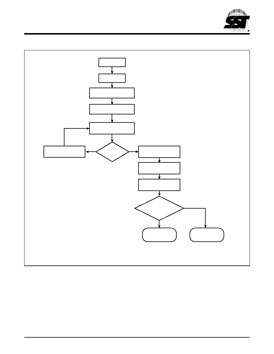
FIGURE 13: C
HIP
-E
RASE
A
LGORITHM
FOR
SST27SF256
Start
VPP = VPPH, A9 = VH
VPP = VDD or VSS
A9 = VIL or VIH
Wait for VPP and A9
Recovery Time
Erase 100ms pulse
(CE# = VIL)
Read Device
(CE# = OE# = VIL)
Device Passed
Compare All
bytes to FFH
Device Failed
1152 F08a.2
No
Yes

18
Data Sheet
256 Kbit / 512 Kbit / 1 Mbit / 2 Mbit Many-Time Programmable Flash
SST27SF256 / SST27SF512 / SST27SF010 / SST27SF020
©2003 Silicon Storage Technology, Inc.
S71152-05-000
9/03
FIGURE 14: C
HIP
-E
RASE
A
LGORITHM
FOR
SST27SF512
OE#/VPP = VPPH
OE#/VPP = VDD or VSS
A9 = VIL or VIH
Wait for OE#/VPP and
A9 Recovery Time
Erase 100ms pulse
(CE# = VIL)
Read Device
(CE# = OE# = VIL)
Device Passed
Compare All
bytes to FFH
Device Failed
1152 F08b.2
Start
A9 = VH
No
Yes
Data Sheet
256 Kbit / 512 Kbit / 1 Mbit / 2 Mbit Many-Time Programmable Flash
SST27SF256 / SST27SF512 / SST27SF010 / SST27SF020
19
©2003 Silicon Storage Technology, Inc.
S71152-05-000
9/03
FIGURE 15: C
HIP
-E
RASE
A
LGORITHM
FOR
SST27SF010/020
Start
A9 = VH, VPP = VPPH
A9 = VIL or VIH
CE# = VIL, OE# = VIH
Wait A9 Recovery Time
Erase 100ms pulse
(PGM# = VIL)
Read Device
Device Passed
Compare all
bytes to FFH
Device Failed
1152 F08c.1
PGM# = VIH
No
Yes
20
Data Sheet
256 Kbit / 512 Kbit / 1 Mbit / 2 Mbit Many-Time Programmable Flash
SST27SF256 / SST27SF512 / SST27SF010 / SST27SF020
©2003 Silicon Storage Technology, Inc.
S71152-05-000
9/03
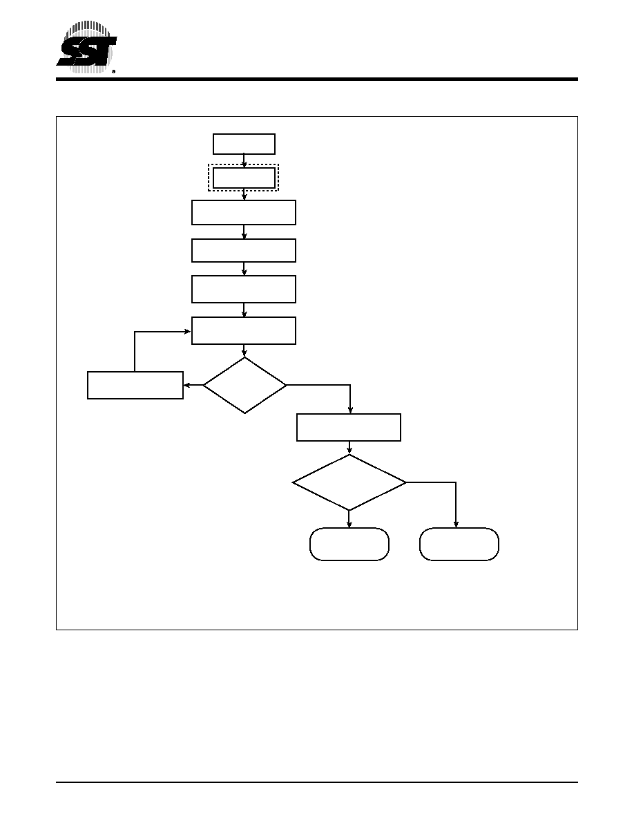
FIGURE 16: B
YTE
-P
ROGRAM
A
LGORITHM
FOR
SST27SF256
Start
Erase*
VPP = VPPH
Address = First Location
Program 20µs pulse
(CE# = VIL)
Read Device
(CE# = OE# = VIL)
Device Passed
Compare all bytes
to original data
Increment Address
Device Failed
1152 F09a.3
Last Address?
Wait for VPP
RecoveryTime
VPP = VDD or VSS
No
No
Yes
Yes
* See Figure 13
Data Sheet
256 Kbit / 512 Kbit / 1 Mbit / 2 Mbit Many-Time Programmable Flash
SST27SF256 / SST27SF512 / SST27SF010 / SST27SF020
21
©2003 Silicon Storage Technology, Inc.
S71152-05-000
9/03
FIGURE 17: B
YTE
-P
ROGRAM
A
LGORITHM
FOR
SST27SF512
Start
Erase*
OE#/VPP = VPPH
Address = First Location
Program 20µs pulse
(CE# = VIL)
Read Device
(CE# = OE# = VIL)
Device Passed
Compare all bytes
to original data
Increment Address
Device Failed
1152 F09b.2
Last Address?
Wait for OE#/VPP
RecoveryTime
OE#/VPP = VDD or VSS
No
No
Yes
Yes
* See Figure 14
22
Data Sheet
256 Kbit / 512 Kbit / 1 Mbit / 2 Mbit Many-Time Programmable Flash
SST27SF256 / SST27SF512 / SST27SF010 / SST27SF020
©2003 Silicon Storage Technology, Inc.
S71152-05-000
9/03
FIGURE 18: B
YTE
-P
ROGRAM
A
LGORITHM
FOR
SST27SF010/020.
Start
Erase*
VPP = VPPH
Address = First Location
CE# = VIL, OE# = VIH
Program 20µs pulse
(PGM# = VIL)
Read Device
Device Passed
Compare all bytes
to original data
Increment Address
Device Failed
1152 F09c.1
Last Address?
No
No
Yes
Yes
* See Figure 15
Data Sheet
256 Kbit / 512 Kbit / 1 Mbit / 2 Mbit Many-Time Programmable Flash
SST27SF256 / SST27SF512 / SST27SF010 / SST27SF020
23
©2003 Silicon Storage Technology, Inc.
S71152-05-000
9/03
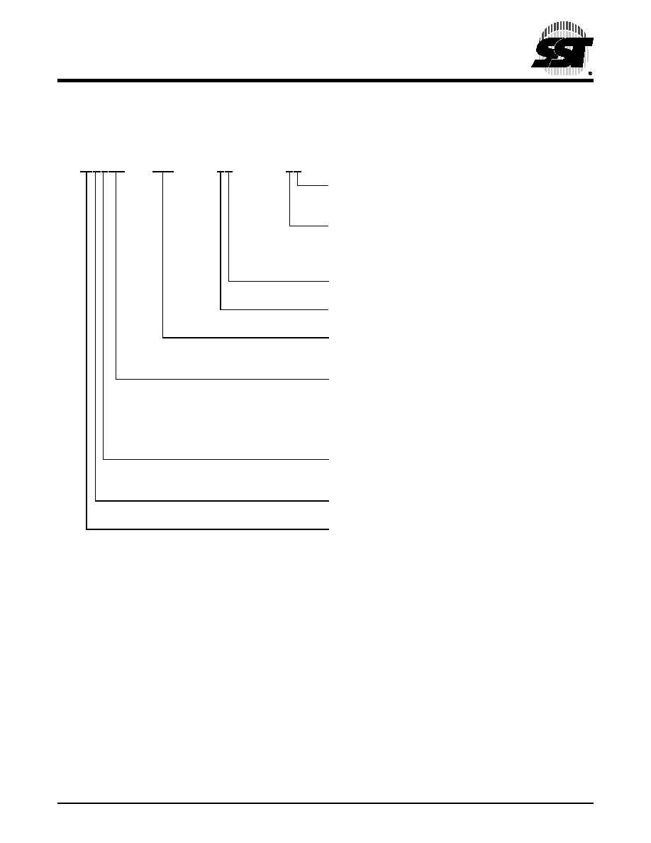
PRODUCT ORDERING INFORMATION
Device
Speed
Suffix1
Suffix2
SST27SFxxx
-
XXX
-
XX
-
XX
Package Modifier
G = 28 pins
H = 32 pins or leads
Package Type
N = PLCC
P = PDIP
W = TSOP (type 1, die up, 8mm x 14mm)
Temperature Range
C = Commercial = 0∞C to +70∞C
Minimum Endurance
3 = 1,000 cycles
Read Access Speed
70 = 70 ns
90 = 90 ns
Device Density
x8 Organization
020 = 2 Mbit
010 = 1 Mbit
512 = 512 Kbit
256 = 256 Kbit
Function
F = Chip-Erase
Byte-Program
Voltage Range
S = 4.5-5.5V
Device Family
27 = Many-Time Programmable Flash
24
Data Sheet
256 Kbit / 512 Kbit / 1 Mbit / 2 Mbit Many-Time Programmable Flash
SST27SF256 / SST27SF512 / SST27SF010 / SST27SF020
©2003 Silicon Storage Technology, Inc.
S71152-05-000
9/03
Valid combinations for SST27SF256
SST27SF256-70-3C-NH
SST27SF256-70-3C-WH
SST27SF256-70-3C-PG
SST27SF256-90-3C-NH
SST27SF256-90-3C-WH
SST27SF256-90-3C-PG
Valid combinations for SST27SF512
SST27SF512-70-3C-NH
SST27SF512-70-3C-WH
SST27SF512-70-3C-PG
SST27SF512-90-3C-NH
SST27SF512-90-3C-WH
SST27SF512-90-3C-PG
Valid combinations for SST27SF010
SST27SF010-70-3C-NH
SST27SF010-70-3C-WH
SST27SF010-70-3C-PH
SST27SF010-90-3C-NH
SST27SF010-90-3C-WH
SST27SF010-90-3C-PH
Valid combinations for SST27SF020
SST27SF020-70-3C-NH
SST27SF020-70-3C-WH
SST27SF020-70-3C-PH
SST27SF020-90-3C-NH
SST27SF020-90-3C-WH
SST27SF020-90-3C-PH
Note:
Valid combinations are those products in mass production or will be in mass production. Consult your SST sales
representative to confirm availability of valid combinations and to determine availability of new combinations.
Data Sheet
256 Kbit / 512 Kbit / 1 Mbit / 2 Mbit Many-Time Programmable Flash
SST27SF256 / SST27SF512 / SST27SF010 / SST27SF020
25
©2003 Silicon Storage Technology, Inc.
S71152-05-000
9/03
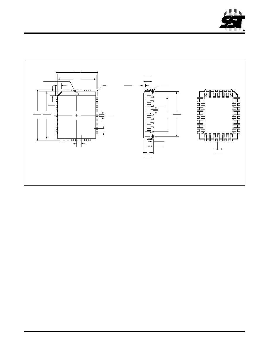
PACKAGING DIAGRAMS
32-
LEAD
P
LASTIC
L
EAD
C
HIP
C
ARRIER
(PLCC)
SST P
ACKAGE
C
ODE
: NH
.040
.030
.021
.013
.530
.490
.095
.075
.140
.125
.032
.026
.032
.026
.029
.023
.453
.447
.553
.547
.595
.585
.495
.485
.112
.106
.042
.048
.048
.042
.015 Min.
TOP VIEW
SIDE VIEW
BOTTOM VIEW
1
2
32
.400
BSC
32-plcc-NH-3
Note: 1. Complies with JEDEC publication 95 MS-016 AE dimensions, although some dimensions may be more stringent.
2. All linear dimensions are in inches (max/min).
3. Dimensions do not include mold flash. Maximum allowable mold flash is .008 inches.
4. Coplanarity: 4 mils.
.050
BSC
.050
BSC
Optional
Pin #1
Identifier
.020 R.
MAX.
R.
x 30∞

26
Data Sheet
256 Kbit / 512 Kbit / 1 Mbit / 2 Mbit Many-Time Programmable Flash
SST27SF256 / SST27SF512 / SST27SF010 / SST27SF020
©2003 Silicon Storage Technology, Inc.
S71152-05-000
9/03
32-
LEAD
T
HIN
S
MALL
O
UTLINE
P
ACKAGE
(TSOP) 8
MM
X
14
MM
SST P
ACKAGE
C
ODE
: WH
32-tsop-WH-7
Note: 1. Complies with JEDEC publication 95 MO-142 BA dimensions,
although some dimensions may be more stringent.
2. All linear dimensions are in millimeters (max/min).
3. Coplanarity: 0.1 mm
4. Maximum allowable mold flash is 0.15 mm at the package ends, and 0.25 mm between leads.
1.20
max.
1mm
Pin # 1 Identifier
12.50
12.30
14.20
13.80
0.70
0.50
8.10
7.90
0.27
0.17
0.50
BSC
1.05
0.95
0.15
0.05
0.70
0.50
0∞- 5∞
DETAIL
Data Sheet
256 Kbit / 512 Kbit / 1 Mbit / 2 Mbit Many-Time Programmable Flash
SST27SF256 / SST27SF512 / SST27SF010 / SST27SF020
27
©2003 Silicon Storage Technology, Inc.
S71152-05-000
9/03
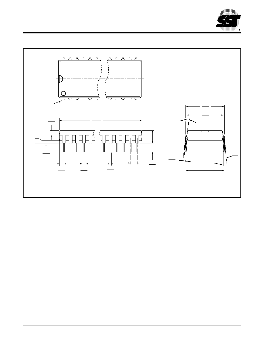
28-
PIN
P
LASTIC
D
UAL
I
N
-
LINE
P
INS
(PDIP)
SST P
ACKAGE
C
ODE
: PG
28-pdip-PG-3
Pin #1 Identifier
CL
28
1
Base
Plane
Seating
Plane
Note: 1. Complies with JEDEC publication 95 MO-015 AH dimensions, although some dimensions may be more stringent.
2. All linear dimensions are in inches (max/min).
3. Dimensions do not include mold flash. Maximum allowable mold flash is .010 inches.
.200
.170
7∞
4 PLCS.
.600 BSC
.100 BSC
.150
.120
.022
.016
.065
.045
.080
.070
.050
.015
.075
.065
1.455
1.445
.012
.008
0∞
15∞
.625
.600
.550
.530
28
Data Sheet
256 Kbit / 512 Kbit / 1 Mbit / 2 Mbit Many-Time Programmable Flash
SST27SF256 / SST27SF512 / SST27SF010 / SST27SF020
©2003 Silicon Storage Technology, Inc.
S71152-05-000
9/03
32-
PIN
P
LASTIC
D
UAL
I
N
-
LINE
P
INS
(PDIP)
SST P
ACKAGE
C
ODE
: PH
Revision History
Number
Description
Date
02
∑
2002 Data Book
Feb 2002
03
∑
Document Control Release (SST Internal): No technical changes
Apr 2002
04
∑
Corrected
I
H
Supervoltage Current for A
9
from 100µA to 200µA in Tables 6, 7, 8, and 9
Jul 2002
05
∑
Corrected the Test Conditions for I
DD
and I
PPR
in Table 6 on page 8
Sep 2003
32-pdip-PH-3
Pin #1 Identifier
CL
32
1
Base
Plane
Seating
Plane
Note: 1. Complies with JEDEC publication 95 MO-015 AP dimensions, although some dimensions may be more stringent.
2. All linear dimensions are in inches (max/min).
3. Dimensions do not include mold flash. Maximum allowable mold flash is .010 inches.
.200
.170
7∞
4 PLCS.
.600 BSC
.100 BSC
.150
.120
.022
.016
.065
.045
.080
.070
.050
.015
.075
.065
1.655
1.645
.012
.008
0∞
15∞
.625
.600
.550
.530
Silicon Storage Technology, Inc. ∑ 1171 Sonora Court ∑ Sunnyvale, CA 94086 ∑ Telephone 408-735-9110 ∑ Fax 408-735-9036
www.SuperFlash.com or www.sst.com