LCD Controller
1 /30
Issue date:10 May, 2000
Syntek Semiconductor Co., Ltd.
STK55C2081
Specification
1. CHIP FEATURES :
* Operating voltage : 2.5V-6.5V
* Operating current : under 3mA at 3V.
* Dual frequency
- 32.768 KHz for LCD & 0.5 second timer interrupt.
- RC or resonator oscillator for system clock.
- CPU clock is half of system clock.
* Built-in 2K bytes RAM, including LCD display RAM.
* Built-in 64K bytes ROM with 16K bytes per bank.
*Two chip enable signals. One can be expanded to 512K bytes with 16K per bank, and
the other one can be expanded to 2M bytes with 16K per bank.
* One 0.5 second pre-divider timer interrupt with start/stop control.
* 2 output ports for key matrices
- 14 pins for port 1, also used as address pins.
- 4 input pins with wake-up interrupt for port 2.
- Built-in pull-up resistors for port 2.
* 8-bit timer with 8-bit prescale counter, both are auto-reloadable.
* 8-bit sound generator with 8-bit prescaler, both are auto-reloadable.
* Two LCD modes
- LCD mode 1 : 80 segments, 16 commons, 1/5 bias, 1/16 duty and 64 Hz frame
frequency.
- LCD mode 2 : 65 segments, 32 commons, 1/5 bias, 1/32 duty and 64 Hz frame
frequency.
* Selectable 64 Hz Interrupt by NMI.
* Timers and port 2 enable IRQ Interrupt.
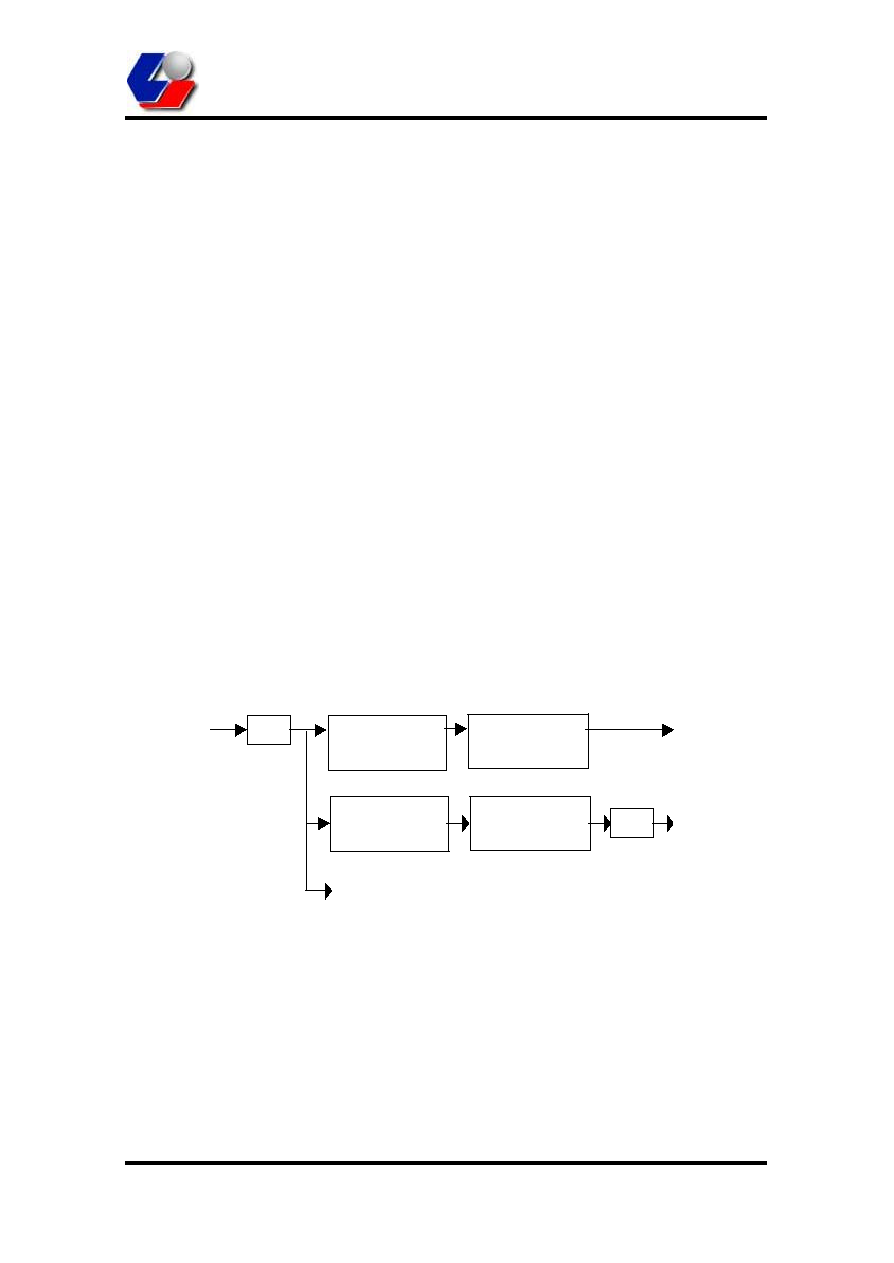
System
clock
1/2
8-bit counter
(prescaler)
8-bit counter
(timer)
IRQ1
CPU clock
8-bit counter
(prescaler)
8-bit counter
(timer)
1/2
SOUND

LCD Controller
2 /30
Issue date:10 May, 2000
Syntek Semiconductor Co., Ltd.
STK55C2081
* Timer range is programmable.
* One output for the speaker.
- 2 KHz or 4 KHz signal with two different envelopes are selectable for sound output.
* One UART serial port with even parity check bit added after MSB for error detecting.
* The internal ROM can be disabled and the corresponding memory area are mapped to
the highest banks of external ROM.
* Sleep mode : LCD off , crystal & system oscillator stop, Vdd=3V, Idd < 1
µ
A.
Stand-by mode : LCD on and system oscillator stop, Vdd=3V, Idd < 80
µ
A. LCD off
and system oscillator stop, Vdd=3V, Idd < 8
µ
A.
2. APPLICATION:
l
Data Bank
l
Translator
l
Organizer
l
Hand-held game
LCD Controller
3 /30
Issue date:10 May, 2000
Syntek Semiconductor Co., Ltd.
STK55C2081
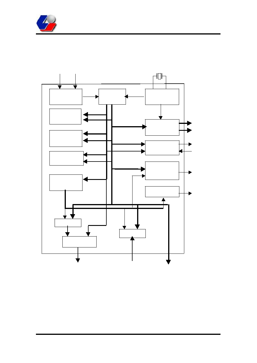
3. BLOCK DIAGRAM:
A0-A15
D0-D7
A0-A13
P20-P23
D0-D7
8-bit CPU
Address
decoder
ROM
64Kx8
RAM
2Kx8
Clock
Generator
LCD driver
Sound
generator
Port 1
Port 2
RC oscillator
SOUND
32768Hz
C1-C32
S1-S65
OSC1
OSC2
UART
MUX
16-bit Timer
TX
RX
Bank control
B0-B6

LCD Controller
4 /30
Issue date:10 May, 2000
Syntek Semiconductor Co., Ltd.
STK55C2081
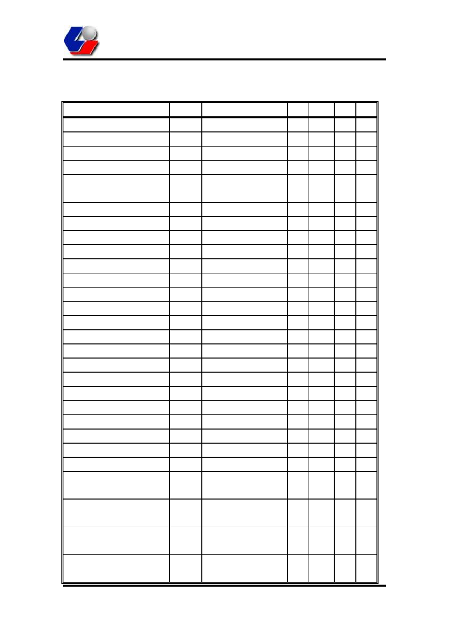
4. PIN DESCRIPTION :
(Total 149 pads)
Pin name
I/O
Description
COM1-COM32
O
Output pins for driving the commons of LCD panel
SEG1-SEG65
O
Output pins for driving the segments of LCD panel
SEG66-SEG80
O
Output pins for driving the segments of LCD panel.
These pins are shared with COM18-COM32.
SOUND
O
Output pin for speaker
A0-A13
O
Address bus outputs shared with port 1 output
L0-L3
IU
4 input pins for key matrix with wake-up interrupt
D0-D7
I/O
Data pins
OSC1
I
RC/Crystal Oscillator input pin for system clock
OSC2
O
RC/Crystal Oscillator output pin for system clock
( Note: CPU clock = system clock/2 )
OSC3
I/O
RC Oscillator bi-directional pin for system clock
/RES
IU
Chip reset
VDD
I
Power input
VSS
I
Signal ground
LOSC1
I
Crystal oscillator input pin
LOSC2
O
Crystal oscillator output pin
BANK0-BANK4
O
To select external memory banks. The data on $1209
will be output in these pins except during /CE2
read/write cycle. At that time these pins will output the
data on $120A
BANK5-BANK6
O
General purpose output pins. Also can be used to
select external memory banks.
/CE1
O
External chip enable 1. This pin will be forced to high
during sleep mode.
/CE2
O
External chip enable 2. This pin will be forced to high
during sleep mode.
/TEST
IU
Test pin. Keep floating or connect to VDD
RWB
O
Read/Write signal output
VLCD
I
Power supply for LCD driver
VR
I
Contrast control for LCD
CLKOUT
O
512 Hz output clock for voltage doubler. This clock
will be stopped if 32.768K Hz crystal is stopped
LCD Controller
5 /30
Issue date:10 May, 2000
Syntek Semiconductor Co., Ltd.
STK55C2081
Pin name
I/O
Description
/DIROM
IU
Internal ROM control pin.
=0 Disable internal ROM
=1 Enable internal ROM
TX
O
Transmit data pin
RX
IU
Receive data pin
Note : IU -- Input pin with pull-up resistor.
5. ADDRESS ARRANGEMENT :
1) RAM
0000-009F : for LCD output data storage while operating in LCD mode 1.
for data area while operating in LCD mode 2.
SEG1-SEG8 SEG9-SEG16
∑
∑
∑
SEG65-SEG72 SEG73-SEG80
COM1
0000
0010
∑
∑
∑
0080
0090
COM2
0001
0011
∑
∑
∑
0081
0091
∑
∑
∑
∑
∑
∑
∑
∑
∑
∑
∑
∑
∑
∑
∑
∑
∑
∑
COM16
000F
001F
∑
∑
∑
008F
009F
* The LSB of low byte - SEG1
The MSB of high byte - SEG80
Middle bits are in order.
00A0-00FF : for zero page area
0100-01FF : for stack area
0200-031F : for data area while operating in LCD mode 1.
for LCD data area while operating in LCD mode 2.
LCD Controller
6 /30
Issue date:10 May, 2000
Syntek Semiconductor Co., Ltd.
STK55C2081
SEG1-SEG8 SEG9-SEG16
∑
∑
∑
SEG57-SEG64
SEG65
COM1
0200
0220
∑
∑
∑
02E0
0300
COM2
0201
0221
∑
∑
∑
02E1
0301
∑
∑
∑
∑
∑
∑
∑
∑
∑
∑
∑
∑
∑
∑
∑
∑
∑
∑
COM32
021F
023F
02FF
031F
* The LSB of low byte - SEG1
The LSB of high byte - SEG65
Middle bits are in order.
0320-07FF : for data area
4000-7FFF : for external chip enable 1. While this area is accessed, /CE1 will be low
and the data in $1209 will be output on BANK0-BANK4. If bit 0 of
$121A is set to one, then this area can not be accessed.
2) ROM
8000-BFFF : for external chip 2 or internal ROM banks.
$121A
/DIROM
Bit 1
Bit 0
Function description
X
0
0
This area is external memory. /CE2 will be low and the data in
$120A will output to BANK0-BANK6.
X
0
1
This condition is prohibited.
0
1
0
This area is external memory. /CE2 will be low and the value
of $1209 will be sent to BANK0-4.
0
1
1
This condition is prohibited.
1
1
X
This area is internal ROM. /CE2 will keep high. $1209
defines the bank number of internal ROM. The internal ROM
are located at bank 1CH-1FH. Bank 00H is used to define
the volume of sound output.

LCD Controller
7 /30
Issue date:10 May, 2000
Syntek Semiconductor Co., Ltd.
STK55C2081
C000-FFFF : for program memory
/DIROM Bit 0 of $121A
Function description
0
0
This area is external memory. /CE2 will be low and BANK4-
BANK0=1FH.
0
1
This condition is prohibited.
1
X
The internal ROM bank 1FH is selected. /CE2 will be high.
FFFF,FFFE - IRQ vector
FFFD,FFFC - RES vector
FFFB,FFFA - NMI vector
3) Others
1200 To enter stand-by mode; write only.
* In standby mode, the system oscillator will be stopped. But 32768Hz crystal
will still work.
* The CPU, UART and timer will be stopped.
* LCD state is depended on bit 1 of $120D.
* NMI and IRQ3 are still functionally.
* When in stand-by mode, NMI, IRQ2 or IRQ3 will wake up the CPU.
1201 To enter sleep mode; write only.
Bit 1 : = 0 Disable sleep mode
= 1 Enable sleep mode
In sleep mode, whole chip will be stopped. That is, the system and 32768 Hz
crystal oscillator will be stopped. The bit 1 of $120D will be reset. Only reset
and IRQ2 will wake up this chip.
1202 Sound output control
Bit 0 : For base frequency
1/32 duty
1/16 duty
= 0 4 KHz
2 KHz
= 1 8 KHz
4 KHz
2-1 : = 0x Sound off
= 10 For alarm envelope
= 11 Sound always on
LCD Controller
8 /30
Issue date:10 May, 2000
Syntek Semiconductor Co., Ltd.
STK55C2081
* The default value for each bit is zero.
Alarm envelope waveform: (unit = second)
1203 IRQ flag register; read & write.
* Read :
Bit 0 : if 1, timer interrupt, IRQ1.
Bit 1 : if 1, port 2 interrupt, IRQ2.
Bit 2 : if 1, 0.5 sec. timer interrupt, IRQ3.
Bit 3 : if 1, transmit data complete interrupt, IRQ4.
Bit 4 : if 1, receiver data ready interrupt, IRQ5.
* Write :
Bit 0 : if 0, clear the flag of IRQ1.
Bit 1 : if 0, clear the flag of IRQ2.
Bit 2 : if 0, clear the flag of IRQ3.
Bit 3 : if 0, clear the flag of IRQ4.
Bit 4 : if 0, clear the flag of IRQ5.
* When the system is in IRQ mode, the IRQ flag register must be cleared
before having another interrupt request; otherwise, the system will always be in
IRQ mode.
1204 Low byte data for port 1; write only.
The output data pins are shared with A0-A7.
1205 High byte data for port 1; write only.
Bit 5-0 : Output data. The output data pins are shared with A8-A13.
1206 Write: load prescaler value and timer value from buffer to counter
Read : read current counter value
* After $1206 been written, timer will begin to count down. And IRQ1
happens when timer counts to zero.
elapsed time = $120B*($120C+1)/(system clock/2).
1207 Port 2 data; read only
Bit 3-0 : Input data . One wait state will be added while reading this port.
1/4
10/16
1/16
1/16

LCD Controller
9 /30
Issue date:10 May, 2000
Syntek Semiconductor Co., Ltd.
STK55C2081
1208 Set port 2 bit interrupt function; write only.
* An '0' in this register will set the interrupt function of the corresponding pin of
port 2 to be enabled.
* The port 2 interrupt is enabled only during sleep or standby mode.
* The default value for each bit is one.
1209 For selecting the memory bank of external chip 1 or internal ROM; write only
Bit 4-0 : set bank number of external chip 1.
120A For selecting the memory bank of external chip 2; write only
Bit 4-0 : set bank number of external chip 2.
6-5 : General purpose output data.
120B Write initial timer prescaler value to buffer; write only
120C Write initial timer value to buffer; write only
120D Control register; write only
Bit
0 : = 0 Disable 64 Hz NMI
= 1 Enable 64 Hz NMI (NMI frequency = 64Hz)
1 : = 0 LCD off
= 1 LCD on
2 : = 0 Disable timer
= 1 Enable timer
3 : = 0 Disable IRQ1
= 1 Enable IRQ1
4 : = 0 Operating in LCD mode 1
= 1 Operating in LCD mode 2
The default value is zero.
120E 0.5 sec timer interrupt; write only
Bit 0 : = 0 Stop 0.5 second timer and reset it
= 1 Start 0.5 second timer
When 0.5 second is elapsed, IRQ3 will occur.
120F Select oscillator warm-up time.
LCD Controller
10 /30
Issue date:10 May, 2000
Syntek Semiconductor Co., Ltd.
STK55C2081
Bit 0 : = 0 warm-up time is 4 system clocks, for RC oscillator
= 1 warm-up time is 31.25ms, for crystal oscillator
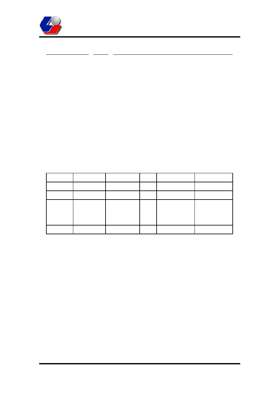
1214 Load baud rate counter value to buffer; write only.
Baud rate = (system clock)/16/([$1214]+1)
Example: For system clock = 2MHz
Baud rate Counter Value (Dec) Actual Baud rate Error (%)
1200
103
1201.92
0.16
2400
51
2403.85
0.16
3600
34
3571.43
-0.79
4800
25
4807.69
0.16
7200
16
7352.94
2.12
9600
12
9615.38
0.16
1215 Load baud rate counter value from buffer to counter to generate desired baud
rate; write only.
1216 Read : read the received data from buffer
Write: load data to buffer for transmission
1217 UART status register; read only.
Bit
0 : = 0 Received data no error
= 1 Received data parity error
1 : = 0 Transmit buffer not ready
= 1 Transmit buffer empty
1218 Write initial prescaler value to sound generator; write only
1219 Write initial value to sound generator; write only
* Output frequency = system clock/[($1219)+1]/[($1218)+1]/4
121A Control register. Write only.
Bit
0 : = 0 Enable external memory expansion. $8000-$BFFF are external
memory. A0-A13 are shared with port 1. D0-D7 are data bus.
= 1 Disable external memory expansion. $8000-$BFFF are internal

LCD Controller
11 /30
Issue date:10 May, 2000
Syntek Semiconductor Co., Ltd.
STK55C2081
ROM. A0-A13 are output port 1 and D0-D7 are data bus.
1 : = 0 $8000-$BFFF are external memory bank.
= 1 $8000-$BFFF are internal ROM bank.
3 : = 0 Select alarm clock output.
= 1 Select sound generator output.
4 : = 0 Disable sound generator.
= 1 Enable sound generator.
The default value is zero.
LCD Controller
12 /30
Issue date:10 May, 2000
Syntek Semiconductor Co., Ltd.
STK55C2081
Bit 3 of $121A
Bit 0 of $1202
2K Hz alarm clock
4K Hz alarm clock
Sound generator output
4) The reset status of CPU
If the /RES is keep low more than two system clocks, then the CPU will be reset.
After reset, the interrupt mask flag is set, the decimal mode is cleared and the program
counter will be loaded with the reset vector from address $FFFC and $FFFD. So,
after initial procedure the firmware should do a `CLI' instruction
. Otherwise, the
CPU will not acknowledge any interrupt.
5) Interrupts
* There are six interrupt sources :
NMI - 64 Hz interrupt
IRQ1 - Timer interrupt
IRQ2 - Sleep and Stand-by interrupts by port 2
IRQ3 - 0.5 second timer interrupt
IRQ4 - Transmit buffer ready interrupt
IRQ5 - Receiver data ready interrupt
* Only IRQ2 will wake up CPU from sleep mode.
* Only IRQ2, IRQ3 and NMI can wake up CPU from stand-by mode.
* An oscillator warm-up time (4 cycles or 31.25ms) will be added before CPU been
waken up from standby or sleep mode.
* After CPU wake up from sleep mode, programmer should turn on LCD again.
* 0.5 sec. timer interrupt, with start/stop control, is operated by writing $120E.
* When port 2 interrupt is enabled, a low signal from any pin will generate IRQ2.
S
0
1
MUX
S
0
1
MUX
SOUND

LCD Controller
13 /30
Issue date:10 May, 2000
Syntek Semiconductor Co., Ltd.
STK55C2081
* Before starting timer, load new prescaler value (by writing $120B) or new timer
value (by writing $120C) to buffer for having different IRQ time ranges. Otherwise,
write $1206 to have the same IRQ time range as the previous one's.
* When the CPU acknowledge the interrupt, following things will be done:
a)
The interrupt mask flag will be set by CPU
b)
The return address and status register will be pushed to stack.
* When the CPU return from interrupt routine by RTI instruction following things will
be done:
a)
The return address and status register will be pulled from stack.
b)
The interrupt mask flag will be cleared.
* It is not necessary to add SEI and CLI instructions in interrupt routine. If a
CLI instruction is added in the interrupt routine, then another interrupt may be
inserted during current interrupt routine and may cause stack overflow.
6) Serial port
* Load baud rate counter value (by writing $1214) to buffer then load it from buffer to
counter( by writing $1215) to generate desired baud rate.
* Write $1216 to transmit data, one byte at a time. When one data byte has been
transmitted, hardware generates IRQ4 interrupt (transmit buffer ready).
* When one data byte is received, hardware generates IRQ5 interrupt (receiver data
ready). Read $1216 to fetch data from buffer.
* Read $1217 bit 0 to check if data received is correct and read bit 1 to check when
next data byte can be transmitted.
* When system is in stand-by mode, serial port is disabled.
7)
Internal ROM.
The internal 64K bytes ROM are split to 4 banks. The bank number is defined by
$1209 and the internal ROM are located at bank 1CH to 1FH. Only bank 1FH can
be read from CPU address 0C000H-0F000H. All the other banks can be read from
8000H-0BFFFH by set $1209 to the bank number and set bit 1 of $121A to one.
8)
Sound volume.
To change the volume, please follow the procedures listed below :
a)
Write zero to $1209.
b)
Set bit 1 of $121A to one.
c)
Set 0 to bit 0 of $8001 to enable the melody output.
LCD Controller
14 /30
Issue date:10 May, 2000
Syntek Semiconductor Co., Ltd.
STK55C2081
d)
Write the volume value to $8000 (bit 0 is do not care).
The default value of volume is $FF.
9) Speech output.
To enable the speech function, please follow the procedures listed below :
a)
Write zero to $1209.
b)
Set bit 1 of $121A to one.
c)
Set 1 to bit 0 of $8001 to disable the melody output and have the DAC always
on.
d)
Change the volume data in $8000 according to the speech data (bit 0 is do not
care).
e)
Repeat a), b) and d) to change the speech data.
f)
After the speech data is finished, repeat procedure a) and b) and then write 0 to
bit 0 of $8001.
g)
Due to the value of $1209 will be changed during speech output, the speech
output program should be located on the $C000-$FFFF area.
(Note : If there is no speech or melody output, then either the bit 0 of $8001 or
$8000 should be kept at zero. Otherwise, a DC current may flow through the
external speaker drive circuit.)
10)
Summary for accessing each bank of memory:
/DIROM Bit 1 of $121A
Bit 0 of $121A
Remarks
0
0
0
$4000 - $7FFF: CE1, bank = ($1209)
$8000 - $BFFF: CE2, bank = ($120A)
$C000 - $FFFF: CE2, bank = $1F
0
0
1
Prohibited
0
1
0
$4000 - $7FFF: CE1, bank = ($1209)
$8000 - $BFFF: CE2, bank = ($1209)
$C000 - $FFFF: CE2, bank = $1F
0
1
1
Prohibited
1
0
0
$4000 - $7FFF: CE1, bank = ($1209)
$8000 - $BFFF: CE2, bank = ($120A)
$C000 - $FFFF: internal, bank = $1F
1
0
1
Prohibited
1
1
0
$4000 - $7FFF: CE1, bank = ($1209)
$8000- $BFFF: internal, bank = ($1209)
LCD Controller
15 /30
Issue date:10 May, 2000
Syntek Semiconductor Co., Ltd.
STK55C2081
/DIROM Bit 1 of $121A
Bit 0 of $121A
Remarks
$C000 - $FFFF: internal, bank = $1F
1
1
1
$4000 - $7FFF: CE1 not accessible
$8000 - $BFFF: internal, bank = ($1209)
$C000 - $FFFF: internal, bank = $1F
LCD Controller
16 /30
Issue date:10 May, 2000
Syntek Semiconductor Co., Ltd.
STK55C2081
$00000
$08000
$0C000
$7FFFF
$78000
Bank $0
Bank $1
Bank $1F
$07FFF
$0FFFF
$77FFF
Bank $1F
$07FFF
$7FFFF
$78000
$0FFFF
$77FFF
Bank $0
Bank $1
$00000
$0C000
$08000
External memory
chip 1
External memory
chip 2
No
implement
Internal ROM
Bank $1F
Bank $1E
Bank $1D
Bank $1C
$1209 defines the
bank number of
this memory if
bit 1 of $121A=1
$120A defines
the bank number
of this memory
$1209 defines
the bank number
of this memory
This memory is
not readable
$1209 defines
the bank number
of this memory
$120A defines
the bank number
of this memory
and $1209 also
defines the bank
number of this
memory if bit 1
of $121A=1
(Always mapped
to CPU address
$8000-$BFFF)
(Always mapped
to CPU address
$4000-$7FFF)
(Always mapped
to CPU address
$8000-$BFFF)
Sound
control
$4000
$00000
$77FFF
$67FFF
$121A
No use
$8000
$07FF
$FFFF
$0000
$6FFFF
$C000
$7FFF
Control port
/DIROM=0
$1200
$78000
Internal
ROM or
External
memory
chip 2
External
memory
chip 1
$60000
$00001
CPU memory mapping
$68000
/DIROM=1
$BFFF
Always read
from bank
$1F
Internal ROM
No use
$70000
$7FFFF
RAM

LCD Controller
17 /30
Issue date:10 May, 2000
Syntek Semiconductor Co., Ltd.
STK55C2081
11)
The sound volume or voice level can only be set at internal $C000-$FFFF bank or
external $C000-$FFFF bank. (Unable to set at $8000- $BFFF bank , whether it is
internal ROM program or external ROM program, also unable to set at $4000-
$7FFF bank).

LCD Controller
18 /30
Issue date:10 May, 2000
Syntek Semiconductor Co., Ltd.
STK55C2081
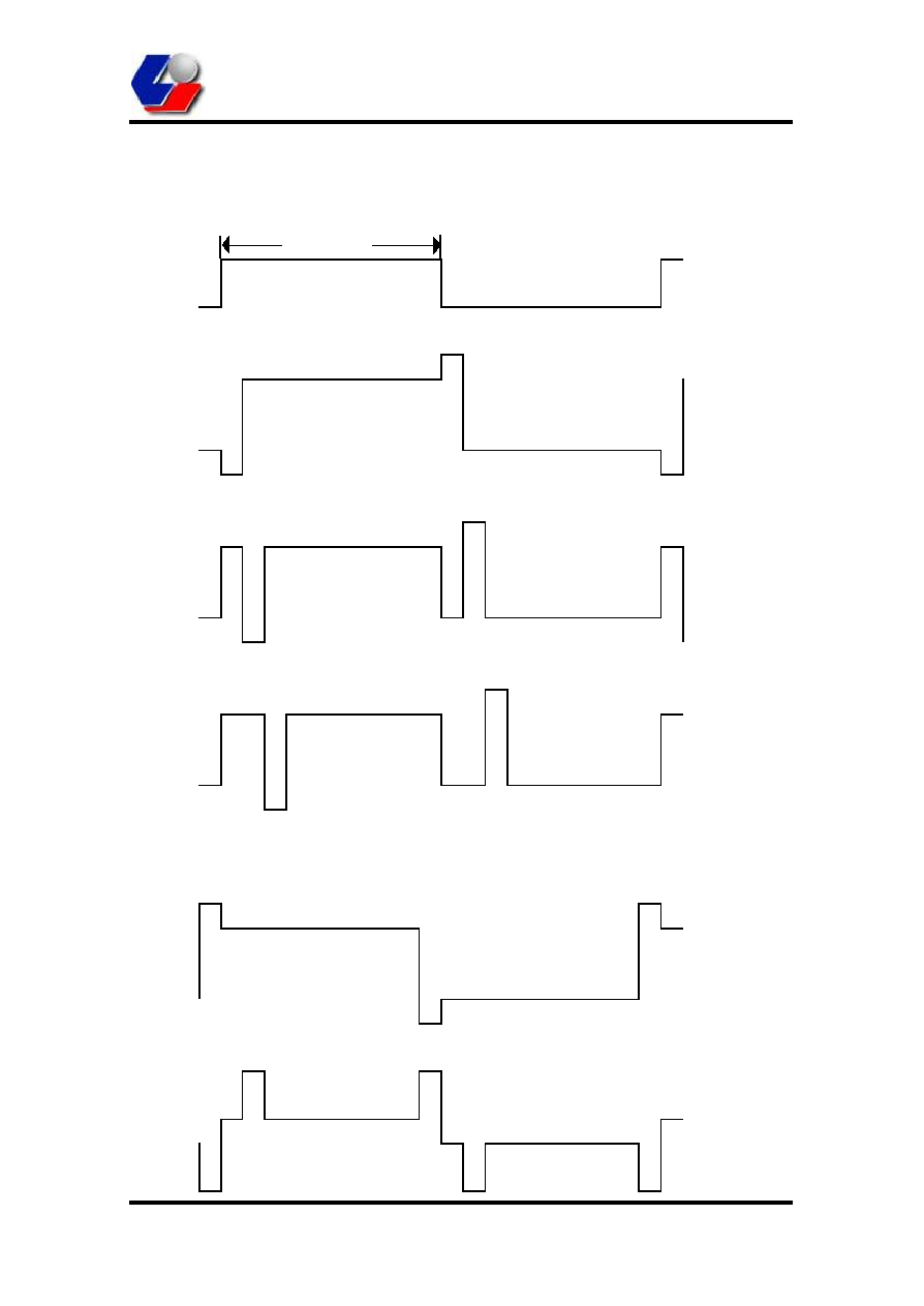
6. I/O STRUCTURE :
6.1 For L0-L3 :
6.2 For output pins :
6.3 /RES pin :
LCD Controller
19 /30
Issue date:10 May, 2000
Syntek Semiconductor Co., Ltd.
STK55C2081
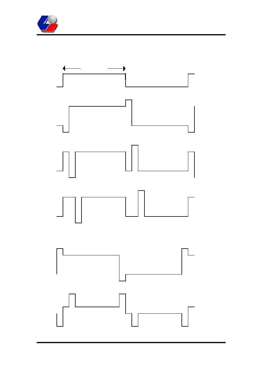
6.4 For I/O pins :
6.5 /DIROM pin :
LCD Controller
20 /30
Issue date:10 May, 2000
Syntek Semiconductor Co., Ltd.
STK55C2081
7. TIMING DIAGRAM FOR EXTERNAL MEMORY ACCESS :
Description
Symbol
Min.
Typ.
Max.
Unit
Cycle Time
Tcyc
500
nS
Address hold time
Tah
10
nS
Address delay time
Tads
100
nS
Delay time
Tdr
10
nS
Write data delay time
Tmds
100
nS
Write data hold time
Tdhw
10
nS
Read data setup time
Tdsr
40
nS
Read data hold time
Tdhr
10
nS
8. ABSOLUTE MAXIMUM RATINGS :
Operating temperature ........................................................... 0 to 70
Storage temperature ......................................................... -65 to 150
Supply voltage ................................................................................. 7 V
Input voltage ............................................................ -0.6 to Vdd+0.6 V
LCD Controller
21 /30
Issue date:10 May, 2000
Syntek Semiconductor Co., Ltd.
STK55C2081
9. ELECTRICAL CHARACTERISTIC :
Parameter
Symbol
Condition
Min Typ. Max Unit
Supply Voltage
Vdd
2.5
3.0 6.5
V
Main system frequency
sys
Vdd=3V
1
5 Mhz
Vdd=4.5V
7 Mhz
Crystal frequency
cry
32768
Hz
Operating current
Idd
Vdd=3V,
sys=1Mhz
1.1
mA
Sleep current
Islp
Vdd=3.5V
1
µ
A
Standby current (LCD on)
Istdby Vdd=2.5V,Vlcd=4V
81
µ
A
Vdd=2.7V,Vlcd=4.5V
97
µ
A
Vdd=3V,Vlcd=5.1V
124
µ
A
Vdd=3.5V,Vlcd=6V
183
µ
A
Vdd=4V, Vlcd=Vdd
83
µ
A
Vdd=4.5V, Vlcd=Vdd
103
µ
A
Vdd=5V, Vlcd=Vdd
124
µ
A
Standby current (LCD off)
Vdd=2.5V
3
µ
A
Vdd=2.7V
3.5
µ
A
Vdd=3V
4.1
µ
A
Vdd=3.5V
5.3
µ
A
Vdd=4V
6.5
µ
A
Vdd=4.5V
8.3
µ
A
Vdd=5V
11
µ
A
Input high voltage
Vih
Vdd=3.0V
1.5
V
Input low voltage
Vil
Vdd=3.0V
-0.6
0.6
V
Input high leakage current
Iih
Vih=Vdd
-1
µ
A
Input low leakage current
Iil
Vil=0
1
µ
A
Output high voltage
(For SEGx and COMx)
Voh1
Ioh=-30
µ
A
Vlcd
-0.2
Vlcd
V
Output low voltage
(for SEGx and COMx)
Vol1
Iol=40
µ
A
0
0.2
V
Output high voltage
(for other pins)
Voh2
Ioh=-4mA
Vdd-
0.8
Vdd
V
Output low voltage
(for other pins)
Vol2
Iol=4mA
0
0.8
V
LCD Controller
22 /30
Issue date:10 May, 2000
Syntek Semiconductor Co., Ltd.
STK55C2081
10. LCD WAVEFORM :
10.1 LCD mode 1 : 80 x 16, 1/5 bias and 1/16 duty
1/64 sec
Vlcd
4/5 Vlcd
3/5 Vlcd
COM1
2/5 Vlcd
1/5 Vlcd
Vss
Vlcd
4/5 Vlcd
3/5 Vlcd
COM2
2/5 Vlcd
1/5 Vlcd
Vss
Vlcd
4/5 Vlcd
3/5 Vlcd
COM3
2/5 Vlcd
1/5 Vlcd
Vss
∑
∑
∑
Vlcd
4/5 Vlcd
3/5 Vlcd
COM16
2/5 Vlcd
1/5 Vlcd
Vss
Vlcd
4/5 Vlcd
3/5 Vlcd
SEGx
2/5 Vlcd
1/5 Vlcd
Vss
LCD Controller
23 /30
Issue date:10 May, 2000
Syntek Semiconductor Co., Ltd.
STK55C2081
There are two LCD matrix DOTs active at (SEGx,COM2) and (SEGx,COM16)
10.2 LCD mode 2 : 65 x 32, 1/5 bias and 1/32 duty
1/64 sec
Vlcd
4/5 Vlcd
3/5 Vlcd
COM1
2/5 Vlcd
1/5 Vlcd
Vss
Vlcd
4/5 Vlcd
3/5 Vlcd
COM2
2/5 Vlcd
1/5 Vlcd
Vss
Vlcd
4/5 Vlcd
3/5 Vlcd
COM3
2/5 Vlcd
1/5 Vlcd
Vss
∑
∑
∑
Vlcd
4/5 Vlcd
3/5 Vlcd
COM32
2/5 Vlcd
1/5 Vlcd
Vss
Vlcd
4/5 Vlcd
3/5 Vlcd
SEGx
2/5 Vlcd
1/5 Vlcd
Vss
There are two LCD matrix DOTs active at (SEGx,COM2) and (SEGx,COM32)
LCD Controller
24 /30
Issue date:10 May, 2000
Syntek Semiconductor Co., Ltd.
STK55C2081
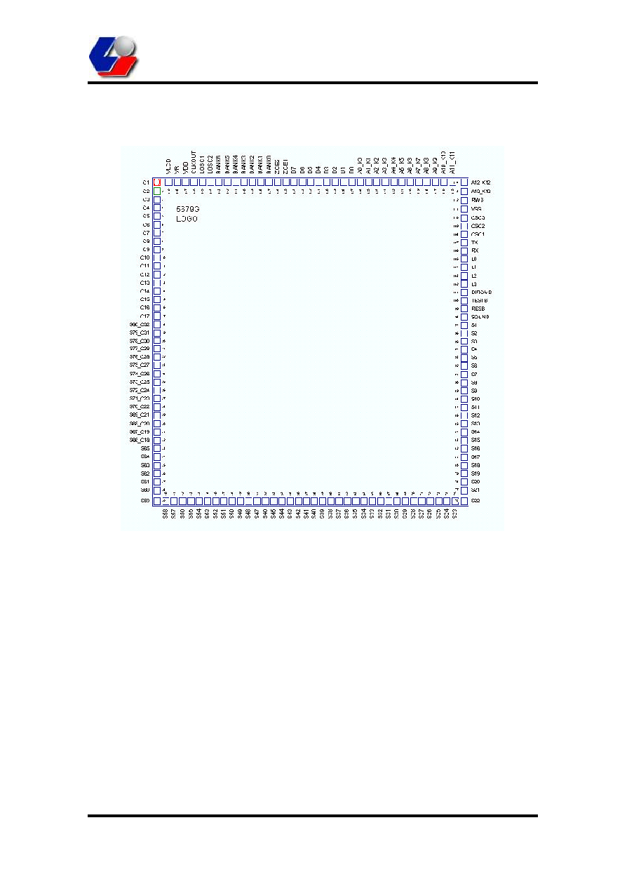
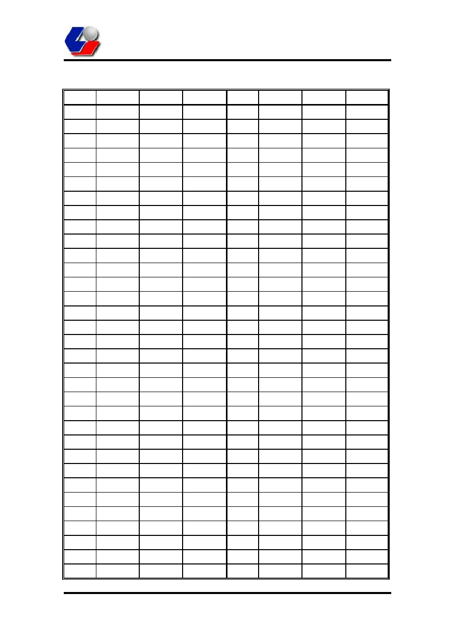
11. PAD LOCATION :
LCD Controller
25 /30
Issue date:10 May, 2000
Syntek Semiconductor Co., Ltd.
STK55C2081
Chip size : 4480 x 4650
Unit :
µ
M
PAD-No
Name
X
Y
PAD-No
Name
X
Y
1
C1
65.00
4585.00
76
S22
4416.00
65.00
2
C2
65.00
4460.00
77
S21
4416.00
218.00
3
C3
65.00
4339.80
78
S20
4416.00
338.00
4
C4
65.00
4222.10
79
S19
4416.00
455.00
5
C5
65.00
4104.40
80
S18
4416.00
572.00
6
C6
65.00
3986.70
81
S17
4416.00
689.00
7
C7
65.00
3869.00
82
S16
4416.00
806.00
8
C8
65.00
3751.30
83
S15
4416.00
923.00
9
C9
65.00
3633.60
84
S14
4416.00
1040.00
10
C10
65.00
3515.90
85
S13
4416.00
1157.00
11
C11
65.00
3398.20
86
S12
4416.00
1274.00
12
C12
65.00
3280.50
87
S11
4416.00
1391.00
13
C13
65.00
3162.80
88
S10
4416.00
1508.00
14
C14
65.00
3045.10
89
S9
4416.00
1625.00
15
C15
65.00
2927.40
90
S8
4416.00
1742.00
16
C16
65.00
2809.70
91
S7
4416.00
1859.00
17
C17
65.00
2692.00
92
S6
4416.00
1976.00
18
S80_C32
65.00
2574.30
93
S5
4416.00
2093.00
19
S79_C31
65.00
2456.60
94
S4
4416.00
2210.00
20
S78_C30
65.00
2338.90
95
S3
4416.00
2327.00
21
S77_C29
65.00
2221.20
96
S2
4416.00
2444.00
22
S76_C28
65.00
2103.50
97
S1
4416.00
2561.00
23
S75_C27
65.00
1985.80
98
SOUND
4416.00
2678.00
24
S74_C26
65.00
1868.10
99
RESB
4416.00
2795.00
25
S73_C25
65.00
1750.40
100
TESTB
4416.00
2912.00
26
S72_C24
65.00
1632.70
101
DIROMB
4416.00
3029.00
27
S71_C23
65.00
1515.00
102
L3
4416.00
3146.00
28
S70_C22
65.00
1397.30
103
L2
4416.00
3263.00
29
S69_C21
65.00
1279.60
104
L1
4416.00
3380.00
30
S68_C20
65.00
1161.90
105
L0
4416.00
3497.00
31
S67_C19
65.00
1044.20
106
RX
4416.00
3614.00
32
S66_C18
65.00
926.50
107
TX
4416.00
3731.00
33
S65
65.00
808.80
108
OSC1
4416.00
3848.00

LCD Controller
26 /30
Issue date:10 May, 2000
Syntek Semiconductor Co., Ltd.
STK55C2081
PAD-No
Name
X
Y
PAD-No
Name
X
Y
34
S64
65.00
691.10
109
OSC2
4416.00
3965.00
35
S63
65.00
573.40
110
OSC3
4416.00
4082.00
36
S62
65.00
455.70
111
VSS
4416.00
4205.60
37
S61
65.00
338.00
112
RWB
4416.00
4330.60
38
S60
65.00
218.00
113
A13_K13
4416.00
4455.60
39
S59
65.00
65.00
114
A12_K12
4416.00
4585.00
40
S58
190.00
65.00
115
A11_K11
4251.00
4585.00
41
S57
310.00
65.00
116
A10_K10
4129.00
4585.00
42
S56
427.00
65.00
117
A9_K9
4011.00
4585.00
43
S55
544.00
65.00
118
A8_K8
3893.00
4585.00
44
S54
661.00
65.00
119
A7_K7
3775.00
4585.00
45
S53
778.00
65.00
120
A6_K6
3657.00
4585.00
46
S52
895.00
65.00
121
A5_K5
3539.00
4585.00
47
S51
1012.00
65.00
122
A4_K4
3421.00
4585.00
48
S50
1129.00
65.00
123
A3_K3
3303.00
4585.00
49
S49
1246.00
65.00
124
A2_K2
3185.00
4585.00
50
S48
1363.00
65.00
125
A1_K1
3067.00
4585.00
51
S47
1480.00
65.00
126
A0_K0
2949.00
4585.00
52
S46
1597.00
65.00
127
D0
2831.00
4585.00
53
S45
1714.00
65.00
128
D1
2713.00
4585.00
54
S44
1831.00
65.00
129
D2
2595.00
4585.00
55
S43
1948.00
65.00
130
D3
2477.00
4585.00
56
S42
2065.00
65.00
131
D4
2359.00
4585.00
57
S41
2182.00
65.00
132
D5
2241.00
4585.00
58
S40
2299.00
65.00
133
D6
2123.00
4585.00
59
S39
2416.00
65.00
134
D7
2005.00
4585.00
60
S38
2533.00
65.00
135
ZCE1
1887.00
4585.00
61
S37
2650.00
65.00
136
ZCE2
1769.00
4585.00
62
S36
2767.00
65.00
137
BANK0
1651.00
4585.00
63
S35
2884.00
65.00
138
BANK1
1533.00
4585.00
64
S34
3001.00
65.00
139
BANK2
1415.00
4585.00
65
S33
3118.00
65.00
140
BANK3
1297.00
4585.00
66
S32
3235.00
65.00
141
BANK4
1179.00
4585.00
67
S31
3352.00
65.00
142
BANK5
1061.00
4585.00
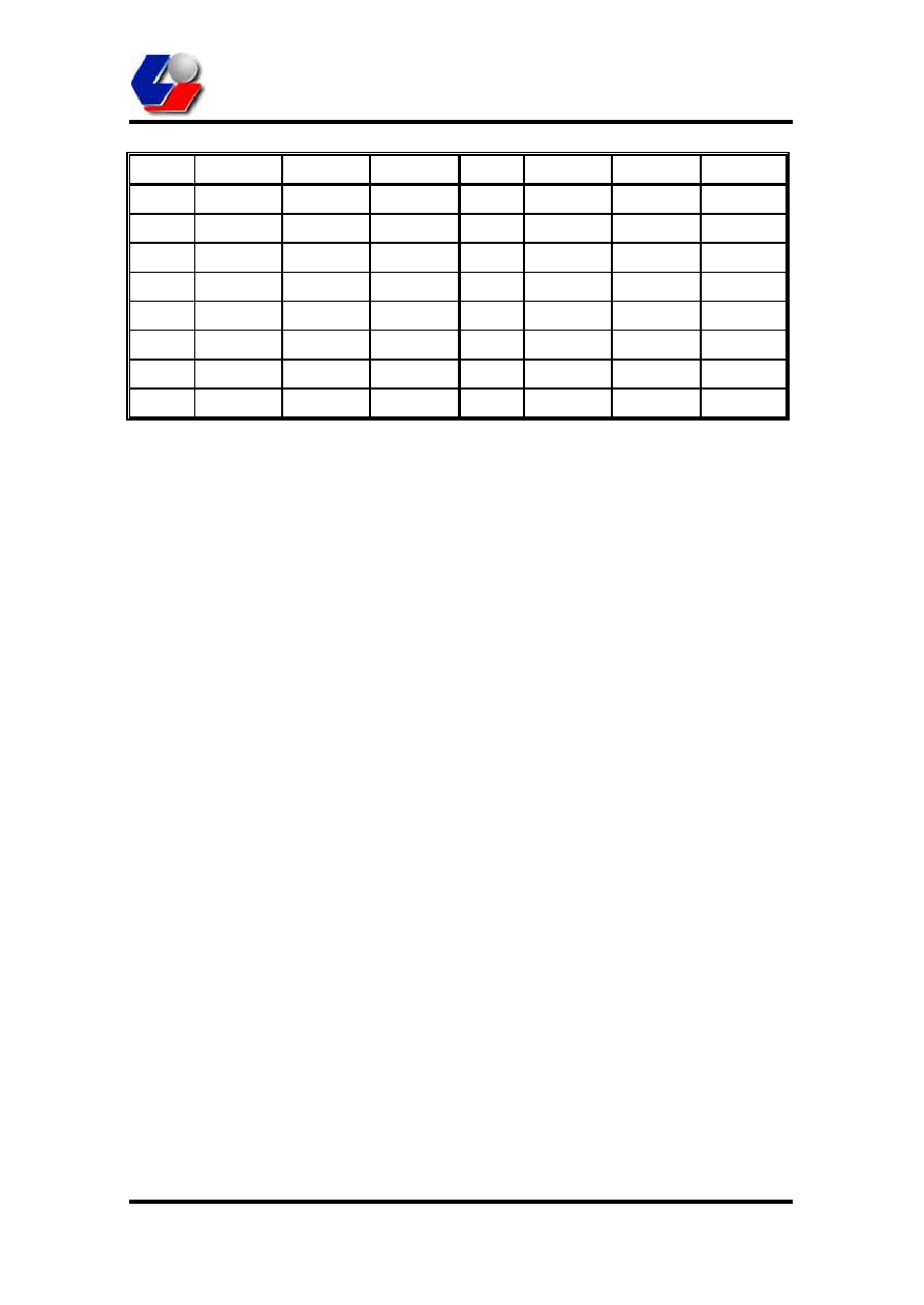
LCD Controller
27 /30
Issue date:10 May, 2000
Syntek Semiconductor Co., Ltd.
STK55C2081
PAD-No
Name
X
Y
PAD-No
Name
X
Y
68
S30
3469.00
65.00
143
BANK6
943.00
4585.00
69
S29
3586.00
65.00
144
LOSC2
825.00
4585.00
70
S28
3703.00
65.00
145
LOSC1
707.00
4585.00
71
S27
3820.00
65.00
146
CLKOUT
589.00
4585.00
72
S26
3937.00
65.00
147
VDD
471.00
4585.00
73
S25
4054.00
65.00
148
VR
353.00
4585.00
74
S24
4171.00
65.00
149
VLCD
230.00
4585.00
75
S23
4291.00
65.00

LCD Controller
29 /30
Issue date:10 May, 2000
Syntek Semiconductor Co., Ltd.
STK55C2081
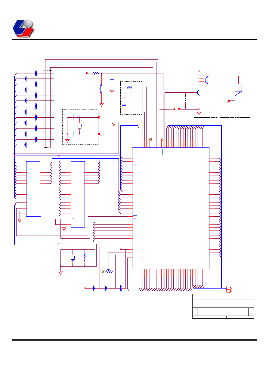
12. APPLICATION CIRCUIT :
STK55C2081
B
Application Circuit
B
1
1
Monday, July 26, 1999
Title
Size
Document Number
Rev
Date:
Sheet
of
VCC
VCC
VCC
VCC
VCC
VCC
OSC1
OSC2
SOUND
For XTAL
For RC
OPEN - Internal ROM
SHORT - External ROM
Key Matrix
Note : Deleted R6 and short VR to VLCD
if contrast control is not needed.
Note :R3 is used to
adjust the sound volume
and can be deleted.
For speaker
For Buzzer
Use 10K ohm
resistor for R3
D0
D1
D2
D3
D4
D5
D6
D7
D0
D1
D2
D3
D4
D5
D6
D7
A10
A9
A8
A7
A6
A5
A4
A3
A2
A1
A0
D0
D1
D2
D3
D4
D5
D6
D7
A0
A1
A2
A3
A4
A5
A6
A7
A8
A9
A10
A11
A12
A13
A0
A1
A2
A3
A4
A5
A6
A7
A8
A9
A10
A11
A12
A13
B0
B1
B2
B3
B4
B0
B0
B1
B2
B3
B4
A1
A0
A2
A3
A4
A5
A6
A7
A8
A9
A10
A11
A12
A13
A13
A12
A11
C2 C3 C4 C5
S65 S64 S63 S62 S61 S60 S59
S50
S51
S52
S53
S54
S55
S56
S57
S58
C23
C12
C9
C24
C26
C14
C25
C15
C17
C31
C16
C10
C22
C6
C28 C27
C32
C21
C30
C8
C13
C29
C11
C7
C20 C19 C18
B5
B6
C1
S35
S43
S33
S14
S8
S1
S45
S34
S29
S26
S4
S41
S22
S17
S39
S37
S32
S27
S3
S47
S42
S36
S28
S19
S2
S46
S40
S30
S20
S5
S49
S48
S38
S15
S7
S6
S24
S18
S11
S21
S12
S31
S16
S10
S9
S23
S44
S25
S13
U3
AM27C040
A0
12
A1
11
A2
10
A3
9
A4
8
A5
7
A6
6
A7
5
A8
27
A9
26
A10
23
A11
25
A12
4
A13
28
A14
29
A15
3
A16
2
A17
30
CE
22
OE
24
A18
31
VPP
1
D0
13
D1
14
D2
15
D3
17
D4
18
D5
19
D6
20
D7
21
U2
MS62256
A0
10
A1
9
A2
8
A3
7
A4
6
A5
5
A6
4
A7
3
A8
25
A9
24
A10
21
A11
23
A12
2
A13
26
A14
1
CE
20
OE
22
WE
27
D0
11
D1
12
D2
13
D3
15
D4
16
D5
17
D6
18
D7
19
Y2
32768Hz
C5
22p
C7
22p
R5
5M
C6
0.1u
+
C8
1u
D16
1N4148
D15
1N4148
D2
1N4148
D3
1N4148
D4
1N4148
D5
1N4148
D6
1N4148
D7
1N4148
D8
1N4148
D9
1N4148
D10
1N4148
D11
1N4148
D12
1N4148
D13
1N4148
D1
1N4148
D14
1N4148
R2
47K
LS1
SPEAKER
Q1
2N8050
R3
R
JP1
C2
22p
C4
22p
C3
5p
R6
500K
C1
0.1u
R1
100K
U1
KC5679
C1
1
C2
2
C3
3
C4
4
C5
5
C6
6
C7
7
C8
8
C9
9
C10
10
C11
11
C12
12
C13
13
C14
14
C15
15
C16
16
C17
17
S80/C32
18
S79/C31
19
S78/C30
20
S77/C29
21
S76/C28
22
S75/C27
23
S74/C26
24
S73/C25
25
S72/C24
26
S71/C23
27
S70/C22
28
S69/C21
29
S68/C20
30
S67/C19
31
S66/C18
32
S65
33
S64
34
S63
35
S62
36
S61
37
S60
38
S59
39
S58
40
S57
41
S56
42
S55
43
S54
44
S53
45
S52
46
S51
47
S50
48
S49
49
S48
50
S47
51
S46
52
S45
53
S42
56
S44
54
S43
55
S41
57
S40
58
S39
59
S38
60
S37
61
S36
62
S35
63
S34
64
S33
65
S32
66
S31
67
S30
68
S29
69
S28
70
S27
71
S26
72
S25
73
S24
74
S23
75
S22
76
S21
77
S20
78
S19
79
S18
80
S17
81
S16
82
S15
83
S14
84
S13
85
S12
86
S11
87
S10
88
S9
89
S8
90
S7
91
S6
92
S5
93
S4
94
S3
95
S2
96
S1
97
SOUND
98
RES
99
TEST
100
DIROM
101
L3
102
L2
103
L1
104
L0
105
RX
106
TX
107
OSC1
108
OSC2
109
OSC3
110
VSS
111
R/W
112
A13/K13
113
A12/K12
114
A11/K11
115
A10/K10
116
A9/K9
117
A8/K8
118
A7/K7
119
A6/K6
120
A5/K5
121
A4/K4
122
A3/K3
123
A2/K2
124
A1/K1
125
A0/K0
126
D0
127
D1
128
D2
129
D3
130
D4
131
D5
132
D6
133
D7
134
CE1
135
CE2
136
BANK0
137
BANK1
138
BANK2
139
BANK3
140
BANK4
141
BANK5
142
BANK6
143
LOSC2
144
LOSC1
145
CLKOUT
146
VDD
147
VR
148
VLCD
149
B Z 1
BUZZER
S1
Y1
CRYSTAL
S[1:65]
C[1:32]

LCD Controller
30 /30
Issue date:10 May, 2000
Syntek Semiconductor Co., Ltd.
STK55C2081
Customer Information Sheet for STK55C2081
971014
1. Customer's Name : ____________________
2. Project title : _________________________
3. Syntek part number : __________________ (will be filled by Syntek)
4. Package -------------------
( ) Chip
( ) QFP
5. Options :
Oscillator type ----------- ( ) RC
( ) XTAL
Operating mode -------- ( ) STK55C2081
( ) STK55C2080
6. Customer code :
Code form ---------------
( ) EPROM
( ) file _______________
Checksum --------------- 0000-3FFF
__________H
4000-7FFF
__________H
8000-BFFF
__________H
C000-FFFF
__________H
0000-FFFF
__________H
7. Operating conditions :
All the operating conditions listed below are for Syntek reference. Syntek will not
guaranty on these values. Please refer to data book or contact Syntek for the guaranty
values.
Operating voltage : _____-_____ V
Voltage doubler : ( ) Yes
( ) No
Operating current : _____ mA
Operating frequency : _____ Hz
Stand-by current : _____
µ
A (LCD On)
_____
µ
A (LCD Off)
Sleep current : _____
µ
A (LCD Off)
Customer : ___________________ Salesman : __________________Date : __/__/__