 | –≠–ª–µ–∫—Ç—Ä–æ–Ω–Ω—ã–π –∫–æ–º–ø–æ–Ω–µ–Ω—Ç: L6245 | –°–∫–∞—á–∞—Ç—å:  PDF PDF  ZIP ZIP |

L6245
5V HARD DISK DRIVE POWER COMBO
PRODUCT PREVIEW
General
+5V OPERATION
REGISTER BASED ARCHITECTURE
MINIMUM EXTERNAL COMPONENTS
SLEEP
AND
IDLE
MODES
FOR
LOW
POWER CONSUMPTION
SELECTABLE GAINS FOR BOTH VCM AND
SPINDLE Gm LOOP
LINEAR CURRENT CONTROL LOOPS FOR
BOTH VCM AND SPINDLE
8 BIT D/A FOR ACTUATOR DRIVER AND
SPINDLE DRIVER
VCM Driver
CURRENT SENSE CONTROL (VOLTAGE
PROPORTIONAL TO CURRENT)
VOLTAGE SENSE CONTROL
(VOLTAGE
PROPORTIONAL
TO
THE
VOLTAGE
ACROSS THE VCM)
TWO CURRENT RANGES FOR SEEKING
AND TRACKING
INTERNAL REGISTER FOR POWER AMP
CONTROL LINES
SPEED
OUTPUT
(VOLTAGE
PROPOR-
TIONAL TO BEMF)
Spindle Driver
BEMF PROCESSING FOR SENSORLESS
MOTOR COMMUTATION
PROGRAMMABLE COMMUTATION PHASE
DELAY
PROGRAMMABLE SLEW-RATE FOR RE-
DUCED EMI
0.7
TYP. FOR ANY HALF BRIDGE
CROSS CONDUCTION PROTECTION
SYNTHESIZED HALL OUTPUT
Other Functions
POWER UP SEQUENCING
POWER DOWN SEQUENCING
LOW VOLTAGE SENSE
ACTUATOR RETRACTION
DYNAMIC BRAKE
THERMAL SHUTDOWN
DESCRIPTION
The L6245 contains in a single chip all the func-
tions to operate a sensorless brushless (DC) mo-
tor and a voice coil motor, suitable for hard disk
drive applications.
The device is configured to interface directly to
an 8 bit parallel microprocessor bus, and has a
register based architecture to reduce number of
interconnection lines. All the positioning loop for
sensorless spindle is integrated, including BEMF
sensing, digital masking, digital delay and se-
quencing. All timing function are performed digi-
tally, thus no external filtering components are re-
quired.
The VCM driver is a transconductance amplifier,
able to provide 2 different current ranges, suitable
for seeking or tracking of the head actuator.
When a low voltage is detected, a monitor, in se-
quence, resets the internal registers, puts in tris-
tate the spindle powers, retracts the actuator, and
applies the dynamic brake of the spindle.
The L6245 is realized in Multipower-BCD 2 tech-
nology, which combine isolate DMOS power tran-
sistors with CMOS and
Bipolar circuits in the
same monolithic layer, and is assembled in a 64-
pin PQFP.
This is advanced information on a new product now in development or undergoing evaluation. Details are subject to change without notice.
October 1992
PQFP64
ORDERING NUMBER: L6245
MULTIPOWER BCD TECHNOLOGY
1/15
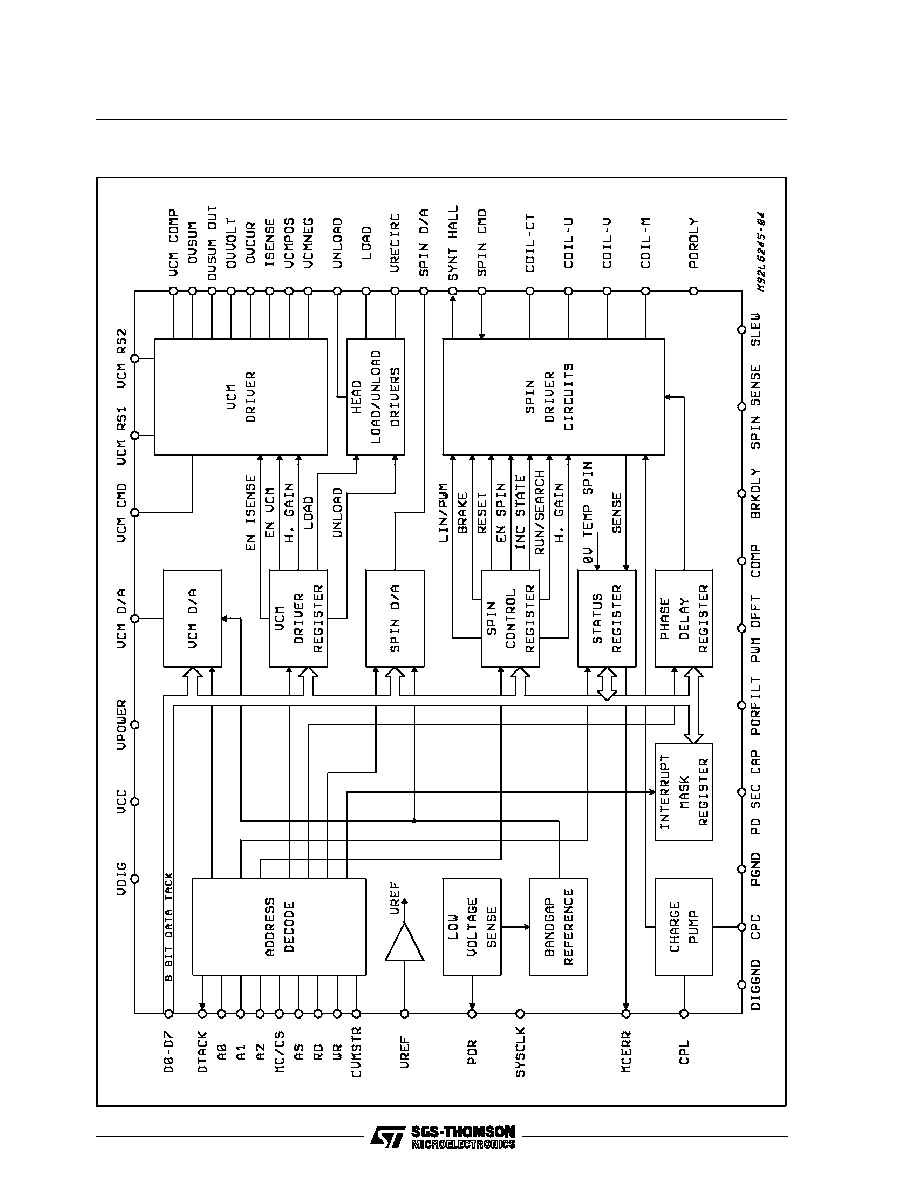
BLOCK DIAGRAM
L6245
2/15

PIN CONNECTION (Top view)
ABSOLUTE MAXIMUM RATINGS
Symbol
Parameter
Value
Unit
V
ds sus
Peak Output Sustaining Voltage
14
V
V
P
; Vcc
Supply Voltage
Power (V
P
)
Logic (V
CC
)
8
6
V
V
V
i
Logic input Voltage
0 to 6
V
V
cp
Charge Pump Input Voltage
18
V
I
p
Sink-Source Peak Output Current
1.5
A
I
O
Sink-Source DC Output Current
1
A
P
tot
Total Power Dissipation (T
amb
= 60
∞
C)
1
W
T
stg,
T
j
Storage and Junction Temperature
≠40 to 150
∞
C
THERMAL DATA
Symbol
Parameter
Value
Unit
R
thj-amb
Thermal Resistance Junction-ambient (*)
max.
90
∞
C/W
(*) Mounted on a typical PCB layout (see Fig. 7)
L6245
3/15
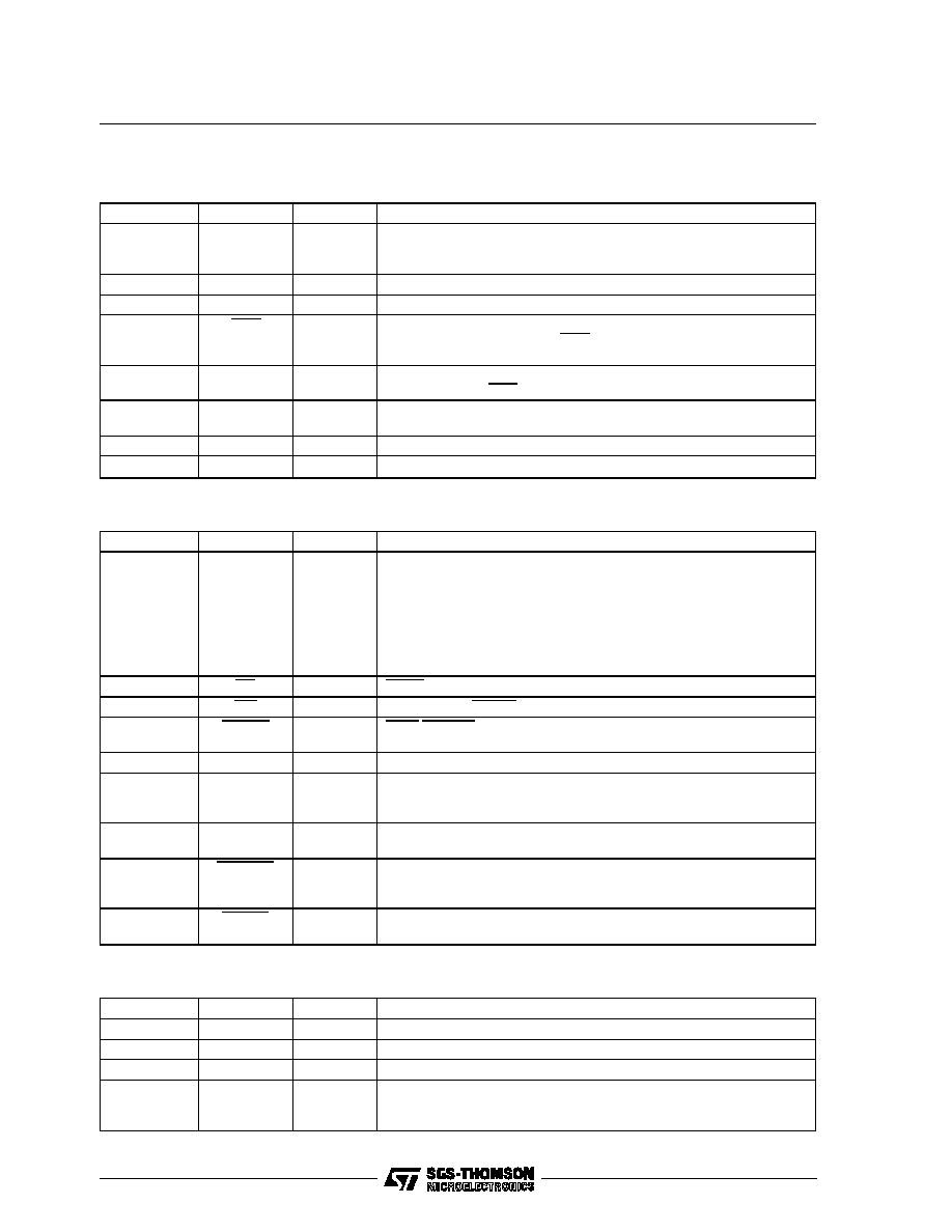
PIN DESCRIPTION [Pin Types: I = Input, O = Output, P = Power, A = Analog (passive)]
Power
Pin Number
Pin Name
Pin Type
Description
12, 17
24,
3
VPOWER
VDIG
V
CC
P
Positive supply, nominally 5V.
7, 42, 64
GND
P
Ground.
10
V
REF
I
All analog signals are referenced to this voltage, nominally 2V.
59
POR
0
POWER ON RESET - Goes low when the supply voltage is below the
VOLTAGE GOOD threshold. POR is an open collector output with an
internal 20k
pull-up.
61
POR_DLY
A
POR DELAY. An external parallel RC network from this pin to ground
sets the time the POR signal stays active after voltage good.
62
POR_FILT
A
An external capacitor from this pin to ground provides filtering for the
V
CC
sense input of the POR circuit.
5
CPC
A
Charge pump capacitor
6
CPL
A
Charge pump inductor
Microprocessor Interface
Pin Number
Pin Name
Pin Type
Description
25
26
27
28
29
30
31
32
D7
D6
D5
D4
D3
D2
D1
D0
I/O
I/O
I/O
I/O
I/O
I/O
I/O
I/O
An 8-bit bidirectional data bus which is connected to the internal
registers.
38
RD
I
READ A low level on this pin allows the bus to be driven by the IC.
39
WR
I
A low level on WRITE allows the IC to read data from the system bus.
35
MC_CS
I
CHIP SELECT A low level on this pin selects the IC for bus
transactions.
41
SYSCLK
I
Microprocessor clock used for internal timing.
33
34
35
A0
A1
A2
I
I
I
The lowest three bits of the system address bus; used to address
internal registers
37
AS
I
ADDRESS STROBE The address appearing on A [0:2] is latched on
the falling edge of the AS pulse.
43
MC_ERR
O
A maskable interrupt signal which is asserted low when an error flag in
the Status Register is set. The output is open-drain with an internal
20K
pull-up.
40
DTACK
O
An open drain, active low signal used for asynchronous bus
transactions.
Brushless, Sensorless Motor Driver and 8 bit D/A
Pin Number
Pin Name
Pin Type
Description
47
SPIN_DAC
O
The output of an 8 bit D/A used for the command to the spindle driver.
48
SPIN_CMD
I
The input to the spindle driver transconductance amplifier.
45
COIL_CT
I
The center tap of the motor is connected to this pin.
53
57
60
COIL_U
COIL_V
COIL_W
O
The motor coils are driven by these outputs. Back EMF is also sensed
at these pins.
L6245
4/15

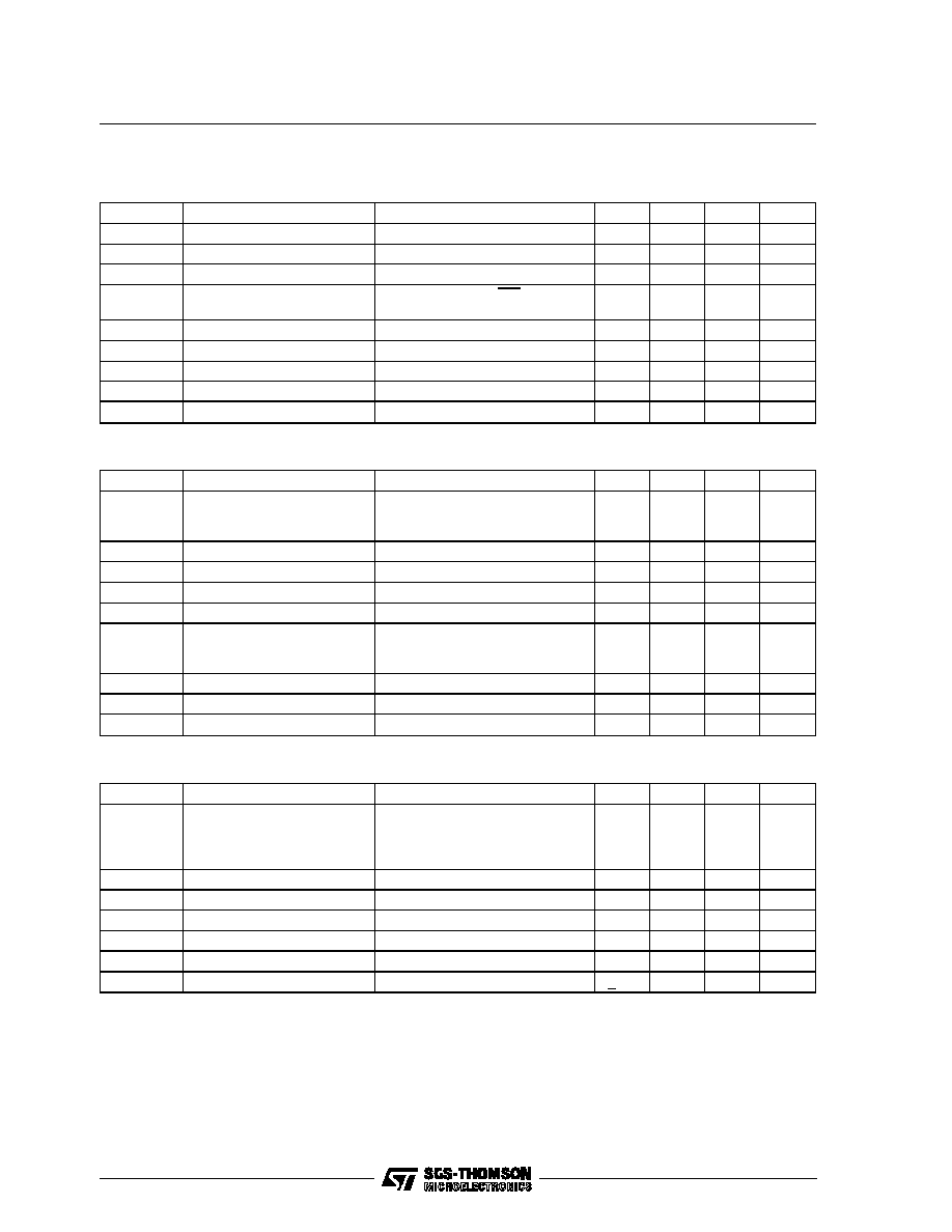
PIN DESCRIPTION (continued)
Pin Number
Pin Name
Pin Type
Description
44
SYNTH_HALL
O
A TTL compatible signal that emulates one of the Hall signals.
SYNTH_HALL is an open drain output with an internal 20K
pull-up.
49, 50,
58
SPIN SENSE
1,2,3
A
The current sensing resistors is connected from these pins to ground.
46
PWM_OFFT
A
A parallel R-C from this pin to ground sets the PWM mode OFF time.
56
SLEW
A
A resistor from this pin to ground sets the slew rate of the driver.
51
S_COMP
A
An R-C network from this pin to GND sets the spin driver
compensation.
VCM Driver and 8 bit D/A
Pin Number
Pin Name
Pin Type
Description
8
VCM_DAC
O
The output of an 8 bit D/A used to command the VCM driver.
9
VCM_CMD
I
VCM driver input command which is relative to V
REF
.
21
VCM_COMP
A
An R-C network from this pin to ground compensates the VCM driver.
14
VCM_RS1
A
The high gain current sense resistor is attached from this pin to ground.
23
VCM_RS2
A
The low gain current sense resistor is connected from this pin to
VCM_RS1
13
VCM+
O
One end of the load is attached to this pin (Positive).
15
VCM-
O
The other end of the load is attached to this pin (Negative).
20
OV_VOLT
O
A voltage which is proportional to the voltage across the load,
referenced to V
REF
.
19
OV_CUR
O
A voltage which is proportional to the current through the load,
referenced to V
REF
.
16
OV_SUM≠
I
Over-velocity summing op-amp inverting input.
18
OV_SUM_OUT
O
Over-velocity summing op-amp output.
22
ISENSE
O
A voltage which is proportional to the current through the VCM load as
sensed by the sense resistor. This signal is enabled by setting bit 2 in
the VCM Control Register.
54
VCM_STRB
I
The 8 bit input to the VCM D/A is updated on the rising edge of
VCM_STRB.
Solenoid Pre-drivers and Power Down Sequencing
Pin Number
Pin Name
Pin Type
Description
11,55,
63
V_RECIR
P
Under normal conditions, power is supplied to various blocks via the
V_RECIR pin. When external power is removed, energy stored in the
rotating spindle is converted to a voltage which supplies the park circuit.
2
LOAD_SOL
O
When a logic one is written to bit 3 of the VCM Control Register,
current is sourced from the LOAD_SOL pin. Otherwise, the pin is high
impedance.
1
UNLOAD_SOL
O
When a logic one is written to bit 4 of the VCM Control Register,
current is sourced from the UNLOAD_SOL pin. Otherwise, the pin is
high impedance.
4
PD_SEQ_CAP
A
When power is removed, the charge stored on this capacitor keeps
selected blocks alive long enough to effect an orderly power down.
52
BRK_DLY
A
An external parallel RC network from this point to ground delays
activation of the dynamic brake after power is removed.
L6245
5/15

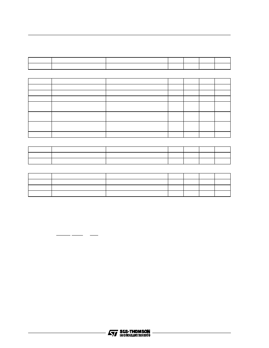
ELECTRICAL CHARACTERISTICS (V
S
= 5V, T
j
= 25
∞
C; unless otherwise specified)
Power Supply Characteristics
Symbol
Parameter
Test Condition
Min.
Typ.
Max.
Units
V
S
Supply Voltage
V
S
= V
P
= V
CC
4.5
5.5
V
ID-READY
ID_IDLE
ID_SLEEP
Quiescent Current Dissipation
No load attached VCM and Spin
drivers enab.
VCM driver disabled Spin driver
enabled
VCM and Spin drivers disabled
25
20
4
mA
mA
mA
VCM Driver (Notes 1, 2)
I
OS
Maximum Load Current
(Seeking)
Output Devices A, B, E, F (Fig. 1)
0.3
A
I
OT
Maximum Load Current
(Traking)
Output Devices C, D (Fig. 1)
0.1
A
R
DS(on)
Source & Sink Out ON
Resistance
Output Devices A, B, E, F
T
j
= 125
∞
C (Fig. 1)
1
R
DS(on)
Sink Out On Resistance
Output Devices C, D
Tj = 125
∞
C (Fig. 1)
2.4
R
DS(on)
Sink Out On Resistance
Parking Device Tj = 125
∞
C
12
V
F
Body Diode Forward Drop
I = 0.3A
1.5
V
V
jump
Jump Discontinuity (**)
R
sense
= 2.01
30
mV
V
DB
Deadband Discontinuity (*)
R
sense
= 2.01
6
mV
V
CMOS
Offset (***)
R
sense
= 2.01
40
mV
(*) The range of input voltages applied to the VCM_CMD pin (with respect to V
REF
) for which only negligible current is present in the load. This
deadband voltage (VDB) can be expressed either in mV or in LSBs, where one LSB is equal to 11.7mV.
(**) A condition in which the transfer characteristic (i.e., load current vs. VCM_CMD-V
REF
) exhibits a slope which is significantly grater than the
desired value. The range of currents for which this condition exists is termed IJUMP. This current is referred o the VCM_CMD input according
to the following equation: VJUMP = IJUMP x 3 x RSENSE
In this document, RSENSE is assumed to be 2.01
. VJUMP can be expressed either in mV or in LSBs, where one LSB is equal to 11.7mV.
(***) The value of VCM_CMD (with respect to V
REF
) for which the load current is zero. In parts which exihibit a DEADBAND dicontinuity, the
offset is defined to be at the midpoint of the deadband region. RSENSE is assumed to br 2.01
.
VCM Current sense amplifier (I
SENSE
)
V
of f
Output Offset Voltage
VCM_RS2 Shorted to GND O/S is
V
(Isense)
- V
ref
≠50
50
mV
G
Closed Loop Voltage Gain
3V/V nominal
2.85
3.15
V/V
PSRR
Power Supply Rejection Ratio
at DC
50
dB
BW
Banwwidth
200
KHz
V
OR
Output Range
V
CC
= 4.5V (note 4)
≠0.2
3.5
V
VCM Full wave rectifying amplifier
I
B
Input Bias Current
VCM_CMD = V
ref
2
µ
A
I
imp
Input Impedance
Impedance seen at VCM_CMD
wrt V
ref
5
K
G
Closed Loop Gain
0.320
0.347
V/V
PSRR
Power Supply Rejection Ratio
at DC
50
dB
GBW
Unity Gain Bandwidth
200
KHz
CMR
Input Common Mode Range
VCM_CMD pin
0.3
3.7
V
V
OR
Output Range
0
1
V
L6245
6/15
ELECTRICAL CHARACTERISTICS (Continued)
VCM DAC (Notes 5, 6)
Symbol
Parameter
Test Condition
Min.
Typ.
Max.
Units
Res
Resolution
8
bit
N.L.
Differential Nonlinearity
±
0.5
LSB
I.N.L.
Integral Nonlinearity
±
0.5
LSB
CT
Conversion Time
From 50% point of WR falling to
1% settling
2
µ
s
Z
O
Output Z
100
FSTC
Full Scale Temp. Coeff.
200
ppm/
∞
C
V
OH
High Output Voltage
Relative to V
ref
Input Code = 7Fh
1.46
1.52
V
V
OL
Low Output Voltage
Relative to Vref Input Code = 80h
≠1.53
≠1.47
V
V
ZSO
Zero Scale Offset
Relative to V
ref
Input Code = 00
±
10
mV
Over velocity detector, coil voltage sense amplifier
Symbol
Parameter
Test Condition
Min.
Typ.
Max.
Units
V
O
Output Offset Voltage
VCM+ = VCM≠, within input
common mode range.
Measure wrt to V
ref
≠50
+50
mV
I
BC
Input Bias Current
(Note 3)
10
µ
A
G
Closed Loop Voltage Gain
Av = 0.25V/V nominal
0.242
0.258
V/V
PSRR
Power Supply Rejection Ratio
at DC
50
dB
BW
Bandwidth
200
KHz
CMR
Input Common Mode Range
Above and below these values
the op amp will be in saturation
and will not invert sign.
0
V
POWER
V
V
DR
Input Differential Range
0
V
POWER
V
V
OR
Output Range
0.3
3.5
V
I
O
Output Current
Ê400
µ
A
Over velocity detector, coil current sense amplifier
Symbol
Parameter
Test Condition
Min.
Typ.
Max.
Units
V
O
Output Offset Voltage
VCM_RS1 shorted to GND for:
(a) VCM_CMD < V
ref
and
b) VCM_CMD > V
ref
. Measure wrt
V
ref
≠50
+50
mV
G
Closed Loop Voltage Gain
Av = 2.5V/V nominal
2.425
2.575
V/V
PSRR
Power Supply Rejection Ratio
at DC
50
dB
Bw
Bandwidth
200
KHz
CMR
Input Common Mode Range
≠0.1
2
V
V
R
Output Range
0.5
3.5
V
I
O
Output Current
+400
mA
L6245
7/15

ELECTRICAL CHARACTERISTICS (Continued)
Over velocity detector, summing amplifier
Symbol
Parameter
Test Condition
Min.
Typ.
Max.
Units
V
O
Input Offset Voltage
10
mV
I
BC
Input Bias Current
1
µ
A
G
Open Loop Gain
60
dB
PSRR
Power Supply Rejection Ratio
at DC
50
dB
GBW
Unity Gain Bandwidth
200
KHz
V
R
Output Range
0.5
3.5
V
I
O
Output Current
+400
µ
A
Over velocity detector, window comparator
Symbol
Parameter
Test Condition
Min.
Typ.
Max.
Units
t
S
Switching Time
50
µ
s
V
TL
Low Threshold
Relative to V
ref
≠1.32
≠1.18
V
V
TH
High Threshold
Relative to Vref
1.18
1.32
V
Solenoid pre-driver (Note 7)
Symbol
Parameter
Test Condition
Min.
Typ.
Max.
Units
I
OH
Output Current
V
OH
= 1.5V, V
CC
= 4.4V
10
mA
Three phase sensorless motor driver
Symbol
Parameter
Test Condition
Min.
Typ.
Max.
Units
I
O
Max. Load Current
0.5
A
R
DS(on)
Out On Resistance
T
j
= 125
∞
C
0.75
dV/dt
Slew Rate
0.05
V/
µ
s
V
F
Body Diode Forward Drop
I = 0.5A
1.2
V
Motor Current Sense Amplifier
Symbol
Parameter
Test Condition
Min.
Typ.
Max.
Units
I
BC
Input Bias Current
1
µ
A
G
Closed Loop Voltage Gain
Low Gain mode
High Gain mode
19.4
4.85
20.6
5.15
V/V
V/V
PSRR
Power Supply Rejection Rate
at DC
50
dB
BW
Bandwidth
200
KHz
I
O
Output Range
0
3.2
V
Spin DAC (Notes 8, 9)
Symbol
Parameter
Test Condition
Min.
Typ.
Max.
Units
Res
Resolution
8
bit
NL
Differential Nonlinearity
±
0.5
LSB
INL
Integral Nonlinearity
±
0.5
LSB
CT
Conversion Time
From 50% point of ≠WR falling to
1% settling
5
µ
s
Zo
Output Z
14
K
FSTC
Full Scale Temp. Coeff.
200
ppm/
∞
C
V
OH
High Output Voltage
2.85
3.15
V
V
OL
Low Output Voltage
Unloaded
0
20
mV
L6245
8/15
FUNCTIONAL DESCRIPTION
Inside the system is the sensorless Spindle driver
(Spin), the Voice Coil Motor driver (VCM), the
Head load/unload predrivers, power sequencing,
actuator over-velocity detection, actuator retrac-
tion and dynamic braking. The architecture of the
system is configured to interface directly to an 8
bit, parallel, microprocessor bus.
During the application of power to the system
(power-on), the output drivers are held in a disabled
state until the applied voltage reaches the Voltage
Good Threshold (VGT). During this period of time
the output drivers are disabled, the internal register
are set to predetermined states, and the Power On
Reset (POR) signal is held low. The POR signal is
held low from the time the applied voltage
reaches 0.7V and the VGT. The POR delay is
programmable changing the value of a capacitor.
The VCM driver is driven via a D/A and it can be
enabled through the VCM driver register. The
VCM driver has a gain capability too. This func-
tion is to be accomplished by switching the sense
resistor used such that the current sensing feed-
back in the VCM driver has more information and
therefore results in lower deadband, offset cur-
rent, and gain error. An actuator over velocity
sensing circuit is incorporated in the system,
which is accomplished by measuring BEMF volt-
age and comparing to a threshold.
ELECTRICAL CHARACTERISTICS (Continued)
Step-up converter
Symbol
Parameter
Test Condition
Min.
Typ.
Max.
Units
V
SU
Step-up Voltage
Relative to V
CC
7
11
V
Microprocessor interface (Note 10)
Symbol
Parameter
Test Condition
Min.
Typ.
Max.
Units
V
IH
High Level Input Voltage
3
V
V
IL
Low Level Input Voltage
0.8
V
V
OH
High Level Output Voltage
VCC = 5V, I
OH
= 400
µ
A
4.4
V
V
OL1
Low Level Output Voltage
≠MCERR, ≠POR, ≠DTACK
IOL = 4mA
0.4
V
V
OL2
Low Level Output Voltage
SYNT_ALL
IOL = 0.5mA
0.4
V
I
IN1
Input Leakage Current
≠RD, ≠WR, AS, ≠MC_CS,
SYSCLK, A [0:2]
1
µ
A
I
IN2
Input Leakage Current
D [0:7]
10
µ
A
Microprocessor interface timing
Trddh
Read Data Hold
5
40
ns
Trddt
≠RD High to ≠DTACK high
40
ns
Twrdt
≠WR High to ≠DTACK High
40
ns
Power on reset
V
CCHL
V
CC
Good, HL
V
CC
falling
4.2
4.4
V
V
CCHL
V
CC
Good, LH
V
CC
rising
4.26
4.5
V
T
PLH
Rise Time
C
Load
= 100pF
200
ns
R
T
Response Time
50
µ
s
Notes:
1) The minimum voltage available from the brushless DC motor after power has been removed is 2.7V
2) The voltage available for actuator etraction shall be greater than 0.7V.
3) Sum of I
bias+
(V
r ef
/internal resistor + power leakage).
4) Minimum output voltage is set to V
ref
by a resistor network.
5) The VCM DAC shall be monotonic over its full range.
6) The coding of the digital input shall be 2's complement.
7) The voltage available for solenoid operation shall be greater than 1.9V.
8) The Spin DAC shall be monotonic over its full range.
9) The coding of the digital input shall be uniplar (unsigned binary).
10) SYNTH_HALL, MC_ERR, DTACK and POR shall have open drain (collector) outputs and internal pull-up resistors. The minimum value of
these pull-up resistors shall be 20K
..
L6245
9/15

The head load /unload mechanisms are just buff-
ers for driving external power transistors. Control-
led internally by Bit 3 and Bit 4 of the VCM Driver
Register, each output has a current surcing capa-
bility of 10mA.
The Sensorless Spindle Driver function can be
accessed from the microprocessor over the data
bus to the Spin Register and Spin D/A. The Spin
D/A is in Binary format. The operation of the Spin-
dle system is controlled entirely by the microproc-
essor from start-up to speed regulaton. The spin
system is accessible by selecting the Spin Control
Register with the address 011 on the 3 bit ad-
dress bus and has the following functions:
1)Enable (Bit 0): high to enable the spin sys-
tem, while a low
asserts braking of the
spindle motor (if VCR enable is low.)
2)Sense amplifier gain (Bit 1): high implies
high current mode which is
equivalent to
low sense amp gain, while a low selects
low current mode
or high sense amp
gain.
3)Unipolar/Bipolar (Bit 2): High selects the
Unipolar driving mode.
4)Run/Search Mode (Bit 3): high selects the
run mode whereby the Hall
synthesizer
output gives speed information while a low
asserts the search mode whereby the se-
quencer is under
µ
P control (stepper func-
tion).
5)Reset State (Bit 4): a low level resets the
commutation state sequencer.
6)Incremental state (Bit 5): toggling of the bit
increments the sequencer
to drive the
output stage when search mode is se-
lected.
7)Linear/PWM (Bit 6): high selects linear
mode of driving for current
(speed) regu-
lation while a low sets to PWM mode used
during start-up.
Start-up current limiting is accomplished by the
output of the microprocessor commanded D/A
value. Jammed or stuck rotor detection is also
done as part of the microprocessor algorithm. In-
tegrated diode are present in the power bridge for
BEMF rectification. This rectified voltage is used
to retract the actuator and unload or latch the
head assembly.
A conventional Bandgap is used to generate in-
ternal biasing for the device as well as the refer-
ence voltage for the D/A converters.
A Step-up Converter is used to generate a 15V
internal supply to drive the upper DMOSs and a
regulated 11.6V internal supply to power internal
circuits which have voltage head room problem,
as well as to drive the lower DMOSs.
A Low Voltage Detector (LVD) is incorporated to
sense a severely low value of applied voltage so
as to shunt-down the VCM and Spindle drivers.
The LVD is activated when the applied voltage
drops below 4.3V (+/-0.1V). When a voltage drop
is sensed, the LVD:
1. asserts POR, which resets the internal register ;
2. retracts the actuator ;
3. applies the dynamic brake.
When a severe low value of applied voltage is
sensed, the motor control system goes into reset
mode and also asserts the POR line to reset
other circuits. The sub-circuit which get affected
by the reset mode in the motor control system are
the Spin Control Register, the VCM Driver Regis-
ter, the Spindle D/A and the VCM D/A. This effec-
tively disables the spin driver, VCM driver, head
load/unload driver and initializes the D/A's at zero
output command value.
An Over Velocity Detector circuit is integrated to
sense when head arms are moving at a speed
which could cause a damaging condition. When
an over velocity condition is detected sensing the
actuator BEMF, the actuator driver is shut off and
held off until the microprocessor has detected this
condition and then resets the error and retries the
access.
The microprocessor has the possibility to put the
device in sleep mode, which is asserted when
both the VCM and Spindle drivers are disabled
through the internal registers (Enable VCM and
Enable Spindle). Under this condition, only the
POR circuit is kept "alive", thus power consump-
tion is kept at minimal. Before sleep mode is acti-
vated, the microprocessor must move the actua-
tor to the unload zone, unload the recording
heads, and apply dynamic braking.
All bits of all the registers are readable by the mi-
croprocessor interface. Also there are certain bits
of the internal registers which are writable as de-
fined in the Register Definition Tables (Tables 1 -
7).
An internal register monitors the internal work of
the system and latches certain error condition that
are detected.
L6245
10/15

REGISTER DEFINITION and 3bit Address Code
Table 1: Status Register (A.C. 001)
Bit
Name
POR Initial
Value
7
6
5
4
3
2
1
0
NC
NC
NC
NC
REVERSE SPIN
OVER TEMP.
SPIN SENSE
OVER VEL SET
1
1
0
1
Table 2: VCM Driver Register (A.C. 010)
Bit
Name
POR Initial
Value
7
6
5
4
3
2
1
0
NC
NC
NC
UNLOAD HD
LOAD HD
ENABLE ISENSE
HIGH GAIN VCM
ENABLE VCM
0
0
0
0
0
Table 3: Spin Control Register (A.C. 011)
Bit
Name
POR Initial
Value
7
6
5
4
3
2
1
0
NC
LINEAR/PWM
INCREMENT STATE
RESET STATE
RUN/SEARCH
UNI/BI
HIGH GAIN SPIN
ENABLE Spin
0
0
0
0
0
0
0
0
Table 4: VCM D/A Register (A.C. 100)
Bit
Name
POR Initial
Value
7
6
5
4
3
2
1
0
Most Significant Bit
Least Significant Bit
0
0
0
0
0
0
0
0
Table 5: Spin D/A Register (A.C. 101)
Bit
Name
POR Initial
Value
7
6
5
4
3
2
1
0
Most Significant Bit
Least Significant Bit
0
0
0
0
0
0
0
0
Table 6: Interrupt Mask Register (A.C. 110)
Bit
Name
POR Initial
Value
7
6
5
4
3
2
1
0
NC
NC
NC
NC
NC
MASK REV Spin
MASK OVER TEMP ERROR
MASK OVER VEL ERROR
0
0
0
Table 7: Phase Delay Register (A.C. 111)
Bit
Name
POR Initial
Value
7
6
5
4
3
2
1
0
NC
NC
NC
NC
Most Significant Bit
Least Significant Bit
0
0
0
0
SYSTEM BUS DESCRIPTION
The system bus is designed as a data acknow-
ledge handshanking bus. At the beginning of the
bus cycle the address and chip select are de-
coded transparently and qualified with read or
write going low. On a read operation, data must
not be driven for 5nsec after read goes low to al-
low the bus to clear. Once data is driven, data ac-
knowledge is driven low to notify the processor
that data is on the bus and ready to be read. The
processor reads the data and responds by raising
read. This is an indication that the processor has
compleated the read and cycle is complete. Data
acknowledge and data must go to high im-
pedence within 20ns to clear the bus for the next
L6245
11/15
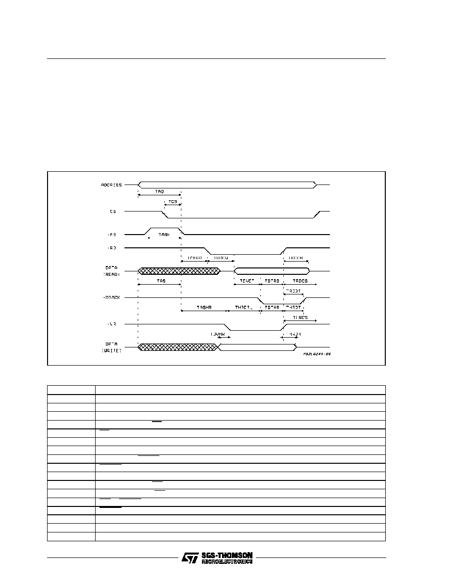
cycle. On a write operation, following write going
low and whatever setup time required to latch
data, data acknwledge is driven low. This notifies
the processor that the cycle can end. This proces-
sor responds by raising write, indicating the end
of the cycle. Data acknowledge must go to high
impedance within 20nsec to clear the bus for the
next cycle.
This handshaking design allows a peripheral to
control the length of the bus cycle. The peripheral
can take as much time as it needs to drive data
onto the bus, then drive DTACK low. Likewise,
the peripheral can wait as long as it needs to set
up data and latch it (or set up data if WR is used
to latch), then drive DTACK low. However, per-
formance is an issue, so even though this control
has been given to the peripheral, it must not be
abused. All delays are minimized to assure opti-
mum system speed, infact the bus can be driven
synchronously (E.G. has regarding DTACK) when
procesor clocks below 12MHz are used.
Figure 1: System Bus Timing (see Table 8)
Table 8: System Bus Timing
Symbol
Description
TAS
Address Setup Time (non MUX bus; (MUX bus)
TCS
System Select to Address Strobe
TASW
Address Strobe Width
TASRD
Address Strobe to RD
TRDDV
RD to Data Driven
TRDDH
Read Data Hold
TRDCS
RD High to CS High
TDVDT
Data Valid to DTACK
TDTRD
DTACK to RD High
TRDDT
RD High to DTACH High
TASWR
Address Strobe to WR
TDVWR
Write Data Valid to WR
TWRDTL
WR to DTACK
TDTWR
DTACK to WR High
TWRCS
WR High to CS High
TWRDT
WR High to DTACK High
TWRDH
Write Data Hold
L6245
12/15

THERMAL CHARACTERISTICS
On the application, the L6245 must be soldered
on a PCB system. The Traks Area, depending on
the lenght and the width of each track, must be
between 2 to 10 square mm. An area of 10 mm
2
can give a typ. Thermal Resistance Junction-to-
Ambient value of 85
∞
C/W (See Fig. 2): this value
refer3 to a Total Power Dissipated Power of 1W.
Fig. 9 shows the increase of the Rth j-amb when
the Dissipated Power decreases.
Practically, very useful information is the change
of the thermal resistance (Thermal Impedance)
versus a single pulse of power width or versus the
time the dissipation begins.
Fig. 4 shows this Thermal Impedance trend.
Figure 2: Typical R
th j-amb
vs. Tracks Area on PCB
Figure 3: Typical Junction-to-Ambient Thermal
Resistance vs. Total Dissipated
Power. (L6245 mounted on a typical
PCB)
Figure 4: Typical Transient Thermal Impedance
vs. Time or Pulse Width. (L6245
mounted on a typical PCB)
L6245
13/15
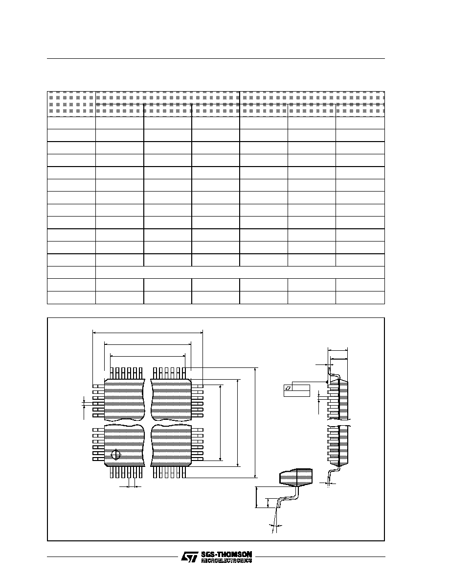
A
A2
A1
B
C
16
17
32
33
48
49
64
E3
D3
E1
E
D1
D
e
1
K
B
PQFP64
L
L1
Seating Plane
0.10mm
PQFP64 PACKAGE MECHANICAL DATA
DIM.
mm
inch
MIN.
TYP.
MAX.
MIN.
TYP.
MAX.
A
3.40
0.134
A1
0.25
0.010
A2
2.55
2.80
3.05
0.100
0.110
0.120
B
0.30
0.45
0.0118
0.0177
C
0.13
0.23
0.005
0.009
D
16.95
17.20
17.45
0.667
0.677
0.687
D1
13.90
14.00
14.10
0.547
0.551
0.555
D3
12.00
0.472
e
0.80
0.0315
E
16.95
17.20
17.45
0.667
0.677
0.687
E1
13.90
14.00
14.10
0.547
0.551
0.555
E3
12.00
0.472
K
0∞
(min.), 7
∞
(max.)
L
0.65
0.80
0.95
0.026
0.0315
0.0374
L1
1.60
0.063
L6245
14/15

Information furnished is believed to be accurate and reliable. However, SGS-THOMSON Microelectronics assumes no responsibility for the
consequences of use of such information nor for any infringement of patents or other rights of third parties which may result from its use. No
license is granted by implication or otherwise under any patent or patent rights of SGS-THOMSON Microelectronics. Specifications men-
tioned in this publication are subject to change without notice. This publication supersedes and replaces all information previously supplied.
SGS-THOMSON Microelectronics products are not authorized for use as critical components in life support devices or systems without ex-
press written approval of SGS-THOMSON Microelectronics.
©
1994 SGS-THOMSON Microelectronics - All Rights Reserved
SGS-THOMSON Microelectronics GROUP OF COMPANIES
Australia - Brazil - France - Germany - Hong Kong - Italy - Japan - Korea - Malaysia - Malta - Morocco - The Netherlands - Singapore -
Spain - Sweden - Switzerland - Taiwan - Thaliand - United Kingdom - U.S.A.
L6245
15/15