 | –≠–ª–µ–∫—Ç—Ä–æ–Ω–Ω—ã–π –∫–æ–º–ø–æ–Ω–µ–Ω—Ç: LK115D00 | –°–∫–∞—á–∞—Ç—å:  PDF PDF  ZIP ZIP |

1/11
February 2003
s
VERY LOW DROPOUT VOLTAGE
(0.2 V TYP.)
s
VERY LOW QUIESCENT CURRENT
(TYP. 0.01µA IN OFF MODE, 280µA IN ON
MODE)
s
OUTPUT CURRENT UP TO 100mA
s
TWO LOGIC-CONTROLLED ELECTRONIC
SHUTDOWNS
s
OUTPUT VOLTAGES OF 2; 2.5; 3.0; 3.3; 4;
4.75; 4.85; 5; 5.5 V
s
INTERNAL CURRENT AND THERMAL LIMIT
s
ONLY 2.2µF FOR STABILITY
s
V
OUT
TOLLERANCE ± 3% AT 25∞C
s
SUPPLY VOLTAGE REJECTION: 80dB (TYP)
s
TEMPERATURE RANGE: -40∞C TO 125∞C
DESCRIPTION
The
LK115D00
series
are
very
Low
Drop
regulators available in SO-8 package and in a
wide range of output voltages.
The very Low Drop voltage (0.2V) and the very
low quiescent current (0.01µA in OFF MODE,
280µA in ON MODE) make them particularly
suitable for Low Noise, Low Power applications
and specially in battery powered systems.
Both active HIGH and active LOW shutdown Logic
Control are available (pin2 and 3). This means
that when the device is used as a local regulator, it
is possible to put a part of the board in standby,
decreasing
the
total
power
consumption.
It
requires only a 2.2 µF capacitor for stability
allowing space and cost saving.
LK115D00
SERIES
VERY LOW DROP WITH INHIBIT
VOLTAGE REGULATORS
SCHEMATIC DIAGRAM
SO-8
LK115D00 SERIES
2/11
ABSOLUTE MAXIMUM RATINGS
Absolute Maximum Ratings are those values beyond which damage to the device may occur. Functional operation under these condition is
not implied.
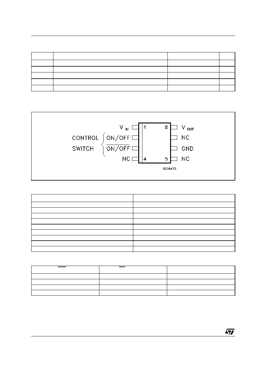
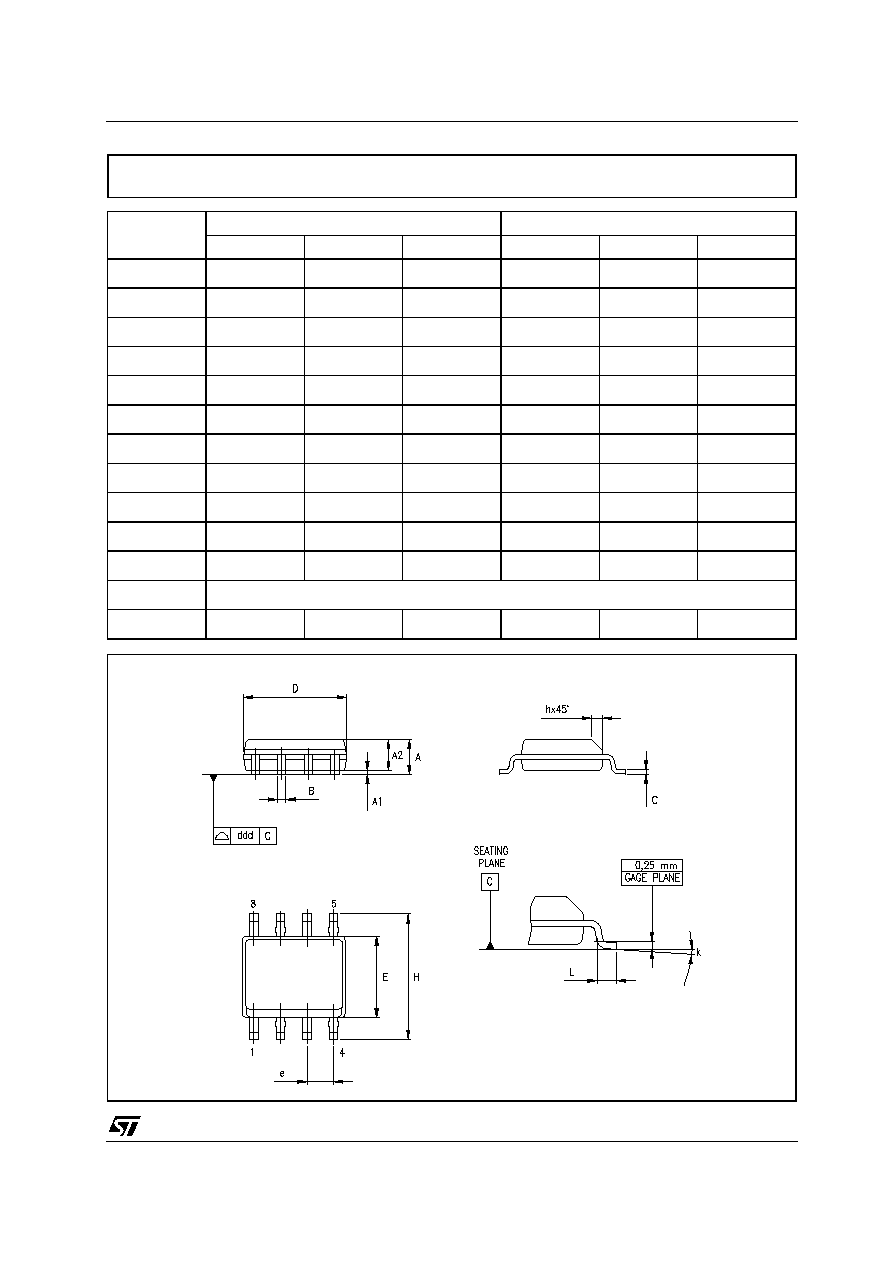
CONNECTION DIAGRAM (top view)
ORDERING CODES
TRUTH TABLE
NOTES: Logic Levels are those defined in the electrical characteristics.
Symbol
Parameter
Value
Unit
V
I
DC Input Voltage
20
V
I
O
Output Current
Internally limited
P
tot
Power Dissipation
Internally limited
T
stg
Storage Temperature Range
-40 to 150
∞C
T
op
Operating Junction Temperature Range
-40 to 125
∞C
TYPE
OUTPUT VOLTAGE
LK115D20
2 V
LK115D25
2.5 V
LK115D30
3 V
LK115D33
3.3 V
LK115D40
4 V
LK115D47
4.75 V
LK115D48
4.85 V
LK115D50
5 V
LK115D55
5.5 V
ON/OFF (PIN 2)
ON/OFF (PIN 3)
STATUS
H
L
ON
H
H
OFF
L
L
OFF
L
H
NOT ALLOWED

LK115D00 SERIES
3/11
TEST CIRCUITS: Supply Current (ON MODE)
TEST CIRCUITS: Supply Current (OFF MODE)
NOTE: The switch emulates the two possibilities to set the regulator in OFF mode.
LK115D00 SERIES
4/11
ELECTRICAL CHARACTERISTICS FOR LK115D20 (refer to the test circuits, T
J
= 25∞C, C
I
= 0.1
µ
F,
C
O
= 2.2
µ
F unless otherwise specified)
ELECTRICAL CHARACTERISTICS FOR LK115D25 (refer to the test circuits, T
J
= 25∞C, C
I
= 0.1
µ
F,
C
O
= 2.2
µ
F unless otherwise specified)
Symbol
Parameter
Test Conditions
Min.
Typ.
Max.
Unit
V
O
Output Voltage
I
O
= 10 mA, V
I
= 4 V
1.940
2
2.060
V
I
O
= 10 mA, V
I
= 4 V, T
a
= -40 to 125
∞C
1.9
2.1
V
I
Operating Input Voltage
I
O
= 100 mA
20
V
I
out
Output Current Limit
120
200
mA
V
O
Line Regulation
V
I
= 3 to 20 V
I
O
=
0.5 mA
2
10
mV
V
O
Load Regulation
V
I
= 3 V
I
O
=
0.5 to 100 mA
4
20
mV
I
d
Quiescent Current
(On Mode)
V
I
= 3 to 20 V
I
O
= 0
0.28
0.5
mA
V
I
= 3 to 20 V
I
O
= 100 mA
1.5
3
(Off Mode)
V
I
= 3 to 20 V
0.01
2
µ
A
SVR
Supply Voltage Rejection
I
O
= 5 mA
V
I
= 4 V ± 1V
f = 120Hz
83
dB
f = 1 KHz
78
f = 10 KHz
59
eN
Output Noise Voltage (RMS)
B = 10 Hz to 100 KHz
44
µ
V
V
d
Dropout Voltage
I
O
= 60 mA
0.17
V
V
HIc
ON/OFF Control (pin 2)
Pin 3 to GND
OFF
0
0.5
V
Pin 3 to GND
ON
2.4
V
in
V
LIc
ON/OFF Control (pin 3)
Pin 2 to
V
in
OFF
V
in
-0.2
V
in
V
Pin 2 to
V
in
ON
0
V
in
-2.4
C
O
Output Bypass Capacitance
ESR = 0.5 to 10
, I
O
=
0 to 100 mA
2
10
µ
F
Symbol
Parameter
Test Conditions
Min.
Typ.
Max.
Unit
V
O
Output Voltage
I
O
= 10 mA, V
I
= 4.5 V
2.425
2.5
2.575
V
I
O
= 10 mA, V
I
= 4.5 V, T
a
= -40 to 125
∞C
2.375
2.625
V
I
Operating Input Voltage
I
O
= 100 mA
20
V
I
out
Output Current Limit
120
200
mA
V
O
Line Regulation
V
I
= 3.5 to 20 V
I
O
=
0.5 mA
2
10
mV
V
O
Load Regulation
V
I
= 3.5 V
I
O
=
0.5 to 100 mA
4
20
mV
I
d
Quiescent Current
(On Mode)
V
I
= 3.5 to 20 V
I
O
= 0
0.28
0.5
mA
V
I
= 3.5 to 20 V
I
O
= 100 mA
1.5
3
(Off Mode)
V
I
= 3.5 to 20 V
0.01
2
µ
A
SVR
Supply Voltage Rejection
I
O
= 5 mA
V
I
= 4.5 V ± 1V
f = 120Hz
81
dB
f = 1 KHz
76
f = 10 KHz
58
eN
Output Noise Voltage (RMS)
B = 10 Hz to 100 KHz
55
µ
V
V
d
Dropout Voltage
I
O
= 60 mA
0.17
V
V
HIc
ON/OFF Control (pin 2)
Pin 3 to GND
OFF
0
0.5
V
Pin 3 to GND
ON
2.4
V
in
V
LIc
ON/OFF Control (pin 3)
Pin 2 to
V
in
OFF
V
in
-0.2
V
in
V
Pin 2 to
V
in
ON
0
V
in
-2.4
C
O
Output Bypass Capacitance
ESR = 0.5 to 10
, I
O
=
0 to 100 mA
2
10
µ
F
LK115D00 SERIES
5/11
ELECTRICAL CHARACTERISTICS FOR LK115D30 (refer to the test circuits, T
J
= 25∞C, C
I
= 0.1
µ
F,
C
O
= 2.2
µ
F unless otherwise specified)
ELECTRICAL CHARACTERISTICS FOR LK115D33 (refer to the test circuits, T
J
= 25∞C, C
I
= 0.1
µ
F,
C
O
= 2.2
µ
F unless otherwise specified)
Symbol
Parameter
Test Conditions
Min.
Typ.
Max.
Unit
V
O
Output Voltage
I
O
= 10 mA, V
I
= 5 V
2.910
3
3.090
V
I
O
= 10 mA, V
I
= 5 V, T
a
= -40 to 125
∞C
2.850
3.150
V
I
Operating Input Voltage
I
O
= 100 mA
20
V
I
out
Output Current Limit
120
200
mA
V
O
Line Regulation
V
I
= 4 to 20 V
I
O
=
0.5 mA
2
10
mV
V
O
Load Regulation
V
I
= 4 V
I
O
=
0.5 to 100 mA
4
20
mV
I
d
Quiescent Current
(On Mode)
V
I
= 4 to 20 V
I
O
= 0
0.28
0.5
mA
V
I
= 4 to 20 V
I
O
= 100 mA
1.5
3
(Off Mode)
V
I
= 4 to 20 V
0.01
2
µ
A
SVR
Supply Voltage Rejection
I
O
= 5 mA
V
I
= 5 V ± 1V
f = 120Hz
79
dB
f = 1 KHz
74
f = 10 KHz
57
eN
Output Noise Voltage (RMS)
B = 10 Hz to 100 KHz
66
µ
V
V
d
Dropout Voltage
I
O
= 60 mA
0.17
V
V
HIc
ON/OFF Control (pin 2)
Pin 3 to GND
OFF
0
0.5
V
Pin 3 to GND
ON
2.4
V
in
V
LIc
ON/OFF Control (pin 3)
Pin 2 to
V
in
OFF
V
in
-0.2
V
in
V
Pin 2 to
V
in
ON
0
V
in
-2.4
C
O
Output Bypass Capacitance
ESR = 0.5 to 10
, I
O
=
0 to 100 mA
2
10
µ
F
Symbol
Parameter
Test Conditions
Min.
Typ.
Max.
Unit
V
O
Output Voltage
I
O
= 10 mA, V
I
= 5.3 V
3.2
3.3
3.4
V
I
O
= 10 mA, V
I
= 5.3 V, T
a
= -40 to 125
∞C
3.135
3.465
V
I
Operating Input Voltage
I
O
= 100 mA
20
V
I
out
Output Current Limit
120
200
mA
V
O
Line Regulation
V
I
= 4.3 to 20 V
I
O
=
0.5 mA
2
10
mV
V
O
Load Regulation
V
I
= 4.3 V
I
O
=
0.5 to 100 mA
4
20
mV
I
d
Quiescent Current
(On Mode)
V
I
= 4.3 to 20 V
I
O
= 0
0.28
0.5
mA
V
I
= 4.3 to 20 V
I
O
= 100 mA
1.5
3
(Off Mode)
V
I
= 4.3 to 20 V
0.01
2
µ
A
SVR
Supply Voltage Rejection
I
O
= 5 mA
V
I
= 5.3 V ± 1V
f = 120Hz
79
dB
f = 1 KHz
74
f = 10 KHz
57
eN
Output Noise Voltage (RMS)
B = 10 Hz to 100 KHz
72.6
µ
V
V
d
Dropout Voltage
I
O
= 60 mA
0.17
V
V
HIc
ON/OFF Control (pin 2)
Pin 3 to GND
OFF
0
0.5
V
Pin 3 to GND
ON
2.4
V
in
V
LIc
ON/OFF Control (pin 3)
Pin 2 to
V
in
OFF
V
in
-0.2
V
in
V
Pin 2 to
V
in
ON
0
V
in
-2.4
C
O
Output Bypass Capacitance
ESR = 0.5 to 10
, I
O
=
0 to 100 mA
2
10
µ
F
LK115D00 SERIES
6/11
ELECTRICAL CHARACTERISTICS FOR LK115D40 (refer to the test circuits, T
J
= 25∞C, C
I
= 0.1
µ
F,
C
O
= 2.2
µ
F unless otherwise specified)
ELECTRICAL CHARACTERISTICS FOR LK115D47 (refer to the test circuits, T
J
= 25∞C, C
I
= 0.1
µ
F,
C
O
= 2.2
µ
F unless otherwise specified)
Symbol
Parameter
Test Conditions
Min.
Typ.
Max.
Unit
V
O
Output Voltage
I
O
= 10 mA, V
I
= 6 V
3.880
4
4.120
V
I
O
= 10 mA, V
I
= 6 V, T
a
= -40 to 125
∞C
3.8
4.2
V
I
Operating Input Voltage
I
O
= 100 mA
20
V
I
out
Output Current Limit
120
200
mA
V
O
Line Regulation
V
I
= 5 to 20 V
I
O
=
0.5 mA
3
15
mV
V
O
Load Regulation
V
I
= 5 V
I
O
=
0.5 to 100 mA
4
20
mV
I
d
Quiescent Current
(On Mode)
V
I
= 5 to 20 V
I
O
= 0
0.28
0.5
mA
V
I
= 5 to 20 V
I
O
= 100 mA
1.5
3
(Off Mode)
V
I
= 5 to 20 V
0.01
2
µ
A
SVR
Supply Voltage Rejection
I
O
= 5 mA
V
I
= 5 V ± 1V
f = 120Hz
77
dB
f = 1 KHz
72
f = 10 KHz
56
eN
Output Noise Voltage (RMS)
B = 10 Hz to 100 KHz
88
µ
V
V
d
Dropout Voltage
I
O
= 60 mA
0.17
V
V
HIc
ON/OFF Control (pin 2)
Pin 3 to GND
OFF
0
0.5
V
Pin 3 to GND
ON
2.4
V
in
V
LIc
ON/OFF Control (pin 3)
Pin 2 to
V
in
OFF
V
in
-0.2
V
in
V
Pin 2 to
V
in
ON
0
V
in
-2.4
C
O
Output Bypass Capacitance
ESR = 0.5 to 10
, I
O
=
0 to 100 mA
2
10
µ
F
Symbol
Parameter
Test Conditions
Min.
Typ.
Max.
Unit
V
O
Output Voltage
I
O
= 10 mA, V
I
= 6.8 V
4.607
4.75
4.892
V
I
O
= 10 mA, V
I
= 6.8 V, T
a
= -40 to 125
∞C
4.513
4.987
V
I
Operating Input Voltage
I
O
= 100 mA
20
V
I
out
Output Current Limit
120
200
mA
V
O
Line Regulation
V
I
= 5.8 to 20 V
I
O
=
0.5 mA
3
15
mV
V
O
Load Regulation
V
I
= 5.8 V
I
O
=
0.5 to 100 mA
4
20
mV
I
d
Quiescent Current
(On Mode)
V
I
= 5.8 to 20 V
I
O
= 0
0.28
0.5
mA
V
I
= 5.8 to 20 V
I
O
= 100 mA
1.5
3
(Off Mode)
V
I
= 5.8 to 20 V
0.01
2
µ
A
SVR
Supply Voltage Rejection
I
O
= 5 mA
V
I
= 6.8 V ± 1V
f = 120Hz
75
dB
f = 1 KHz
70
f = 10 KHz
55
eN
Output Noise Voltage (RMS)
B = 10 Hz to 100 KHz
104.5
µ
V
V
d
Dropout Voltage
I
O
= 60 mA
0.17
V
V
HIc
ON/OFF Control (pin 2)
Pin 3 to GND
OFF
0
0.5
V
Pin 3 to GND
ON
2.4
V
in
V
LIc
ON/OFF Control (pin 3)
Pin 2 to
V
in
OFF
V
in
-0.2
V
in
V
Pin 2 to
V
in
ON
0
V
in
-2.4
C
O
Output Bypass Capacitance
ESR = 0.5 to 10
, I
O
=
0 to 100 mA
2
10
µ
F
LK115D00 SERIES
7/11
ELECTRICAL CHARACTERISTICS FOR LK115D48 (refer to the test circuits, T
J
= 25∞C, C
I
= 0.1
µ
F,
C
O
= 2.2
µ
F unless otherwise specified)
ELECTRICAL CHARACTERISTICS FOR LK115D50 (refer to the test circuits, T
J
= 25∞C, C
I
= 0.1
µ
F,
C
O
= 2.2
µ
F unless otherwise specified)
Symbol
Parameter
Test Conditions
Min.
Typ.
Max.
Unit
V
O
Output Voltage
I
O
= 10 mA, V
I
= 6.9 V
4.705
4.85
4.966
V
I
O
= 10 mA, V
I
= 6.9 V, T
a
= -40 to 125
∞C
4.607
5.093
V
I
Operating Input Voltage
I
O
= 100 mA
20
V
I
out
Output Current Limit
120
200
mA
V
O
Line Regulation
V
I
= 5.9 to 20 V
I
O
=
0.5 mA
3
15
mV
V
O
Load Regulation
V
I
= 5.9 V
I
O
=
0.5 to 100 mA
4
20
mV
I
d
Quiescent Current
(On Mode)
V
I
= 5.9 to 20 V
I
O
= 0
0.28
0.5
mA
V
I
= 5.9 to 20 V
I
O
= 100 mA
1.5
3
(Off Mode)
V
I
= 5.9 to 20 V
0.01
2
µ
A
SVR
Supply Voltage Rejection
I
O
= 5 mA
V
I
= 6.9 V ± 1V
f = 120Hz
75
dB
f = 1 KHz
70
f = 10 KHz
55
eN
Output Noise Voltage (RMS)
B = 10 Hz to 100 KHz
106.7
µ
V
V
d
Dropout Voltage
I
O
= 60 mA
0.17
V
V
HIc
ON/OFF Control (pin 2)
Pin 3 to GND
OFF
0
0.5
V
Pin 3 to GND
ON
2.4
V
in
V
LIc
ON/OFF Control (pin 3)
Pin 2 to
V
in
OFF
V
in
-0.2
V
in
V
Pin 2 to
V
in
ON
0
V
in
-2.4
C
O
Output Bypass Capacitance
ESR = 0.5 to 10
, I
O
=
0 to 100 mA
2
10
µ
F
Symbol
Parameter
Test Conditions
Min.
Typ.
Max.
Unit
V
O
Output Voltage
I
O
= 10 mA, V
I
= 7 V
4.85
5
5.15
V
I
O
= 10 mA, V
I
= 7 V, T
a
= -40 to 125
∞C
4.75
5.25
V
I
Operating Input Voltage
I
O
= 100 mA
20
V
I
out
Output Current Limit
120
200
mA
V
O
Line Regulation
V
I
= 6 to 20 V
I
O
=
0.5 mA
3
15
mV
V
O
Load Regulation
V
I
= 6 V
I
O
=
0.5 to 100 mA
4
20
mV
I
d
Quiescent Current
(On Mode)
V
I
= 6 to 20 V
I
O
= 0
0.28
0.5
mA
V
I
= 6 to 20 V
I
O
= 100 mA
1.5
3
(Off Mode)
V
I
= 6 to 20 V
0.01
2
µ
A
SVR
Supply Voltage Rejection
I
O
= 5 mA
V
I
= 7 V ± 1V
f = 120Hz
75
dB
f = 1 KHz
70
f = 10 KHz
55
eN
Output Noise Voltage (RMS)
B = 10 Hz to 100 KHz
110
µ
V
V
d
Dropout Voltage
I
O
= 60 mA
0.17
V
V
HIc
ON/OFF Control (pin 2)
Pin 3 to GND
OFF
0
0.5
V
Pin 3 to GND
ON
2.4
V
in
V
LIc
ON/OFF Control (pin 3)
Pin 2 to
V
in
OFF
V
in
-0.2
V
in
V
Pin 2 to
V
in
ON
0
V
in
-2.4
C
O
Output Bypass Capacitance
ESR = 0.5 to 10
, I
O
=
0 to 100 mA
2
10
µ
F

LK115D00 SERIES
8/11
ELECTRICAL CHARACTERISTICS FOR LK115D55 (refer to the test circuits, T
J
= 25∞C, C
I
= 0.1
µ
F,
C
O
= 2.2
µ
F unless otherwise specified)
Symbol
Parameter
Test Conditions
Min.
Typ.
Max.
Unit
V
O
Output Voltage
I
O
= 10 mA, V
I
= 7.5 V
5.335
5.5
5.665
V
I
O
= 10 mA, V
I
= 7.5 V, T
a
= -40 to 125
∞C
5.225
5.775
V
I
Operating Input Voltage
I
O
= 100 mA
20
V
I
out
Output Current Limit
120
200
mA
V
O
Line Regulation
V
I
= 6.5 to 20 V
I
O
=
0.5 mA
3
15
mV
V
O
Load Regulation
V
I
= 6.5 V
I
O
=
0.5 to 100 mA
4
20
mV
I
d
Quiescent Current
(On Mode)
V
I
= 6.5 to 20 V
I
O
= 0
0.28
0.5
mA
V
I
= 6.5 to 20 V
I
O
= 100 mA
1.5
3
(Off Mode)
V
I
= 6.5 to 20 V
0.01
2
µ
A
SVR
Supply Voltage Rejection
I
O
= 5 mA
V
I
= 7.5 V ± 1V
f = 120Hz
74
dB
f = 1 KHz
69
f = 10 KHz
55
eN
Output Noise Voltage (RMS)
B = 10 Hz to 100 KHz
121
µ
V
V
d
Dropout Voltage
I
O
= 60 mA
0.17
V
V
HIc
ON/OFF Control (pin 2)
Pin 3 to GND
OFF
0
0.5
V
Pin 3 to GND
ON
2.4
V
in
V
LIc
ON/OFF Control (pin 3)
Pin 2 to
V
in
OFF
V
in
-0.2
V
in
V
Pin 2 to
V
in
ON
0
V
in
-2.4
C
O
Output Bypass Capacitance
ESR = 0.5 to 10
, I
O
=
0 to 100 mA
2
10
µ
F
LK115D00 SERIES
9/11
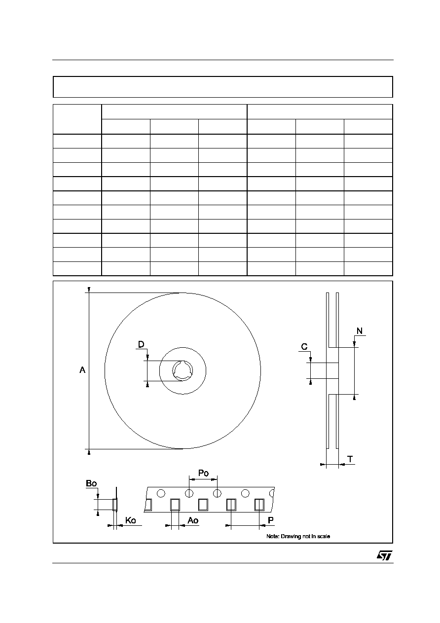
DIM.
mm.
inch
MIN.
TYP
MAX.
MIN.
TYP.
MAX.
A
1.35
1.75
0.053
0.069
A1
0.10
0.25
0.04
0.010
A2
1.10
1.65
0.043
0.065
B
0.33
0.51
0.013
0.020
C
0.19
0.25
0.007
0.010
D
4.80
5.00
0.189
0.197
E
3.80
4.00
0.150
0.157
e
1.27
0.050
H
5.80
6.20
0.228
0.244
h
0.25
0.50
0.010
0.020
L
0.40
1.27
0.016
0.050
k
∞ (max.)
ddd
0.1
0.04
SO-8 MECHANICAL DATA
0016023/C
8
LK115D00 SERIES
10/11
DIM.
mm.
inch
MIN.
TYP
MAX.
MIN.
TYP.
MAX.
A
330
12.992
C
12.8
13.2
0.504
0.519
D
20.2
0.795
N
60
2.362
T
22.4
0.882
Ao
8.1
8.5
0.319
0.335
Bo
5.5
5.9
0.216
0.232
Ko
2.1
2.3
0.082
0.090
Po
3.9
4.1
0.153
0.161
P
7.9
8.1
0.311
0.319
Tape & Reel SO-8 MECHANICAL DATA

LK115D00 SERIES
11/11
Information furnished is believed to be accurate and reliable. However, STMicroelectronics assumes no responsibility for the
consequences of use of such information nor for any infringement of patents or other rights of third parties which may result from
its use. No license is granted by implication or otherwise under any patent or patent rights of STMicroelectronics. Specifications
mentioned in this publication are subject to change without notice. This publication supersedes and replaces all information
previously supplied. STMicroelectronics products are not authorized for use as critical components in life support devices or
systems without express written approval of STMicroelectronics.
© The ST logo is a registered trademark of STMicroelectronics
© 2003 STMicroelectronics - Printed in Italy - All Rights Reserved
STMicroelectronics GROUP OF COMPANIES
Australia - Brazil - Canada - China - Finland - France - Germany - Hong Kong - India - Israel - Italy - Japan - Malaysia - Malta - Morocco
Singapore - Spain - Sweden - Switzerland - United Kingdom - United States.
© http://www.st.com