 | –≠–ª–µ–∫—Ç—Ä–æ–Ω–Ω—ã–π –∫–æ–º–ø–æ–Ω–µ–Ω—Ç: S8C5H30L | –°–∫–∞—á–∞—Ç—å:  PDF PDF  ZIP ZIP |
N-CHANNEL 30V - 0.018
- 8A SO-8
P-CHANNEL 30V - 0.045
- 5A SO-8
LOW GATE CHARGE StripFETTM III MOSFET
1/11
September 2004
STS8C5H30L
Table 1: General Features
s
TYPICAL R
DS(on)
(N-Channel) = 0.018
s
TYPICAL R
DS(on)
(P-Channel) = 0.045
s
CONDUCTION LOSSES REDUCED
s
SWITCHING LOSSES REDUCED
s
LOW THRESHOLD DRIVE
s
STANDARD OUTLINE FOR EASY
AUTOMATED SURFACE MOUNT ASSEMBLY
DESCRIPTION
This MOSFET is the latest development of STMi-
croelectronics unique "Single Feature SizeTM"
strip-based process. The resulting transistor
shows extremely high packing density for low on-
resistance, rugged avalanche characteristics and
less critical alignment steps therefore a remark-
able manufacturing reproducibility.
APPLICATIONS
s
DC/DC CONVERTERS
s
BATTERY MANAGEMENT IN NOMADIC
EQUIPMENT
s
POWER MANAGEMENT IN CELLULAR
PHONES
s
DC MOTOR DRIVE
Table 2: Order Codes
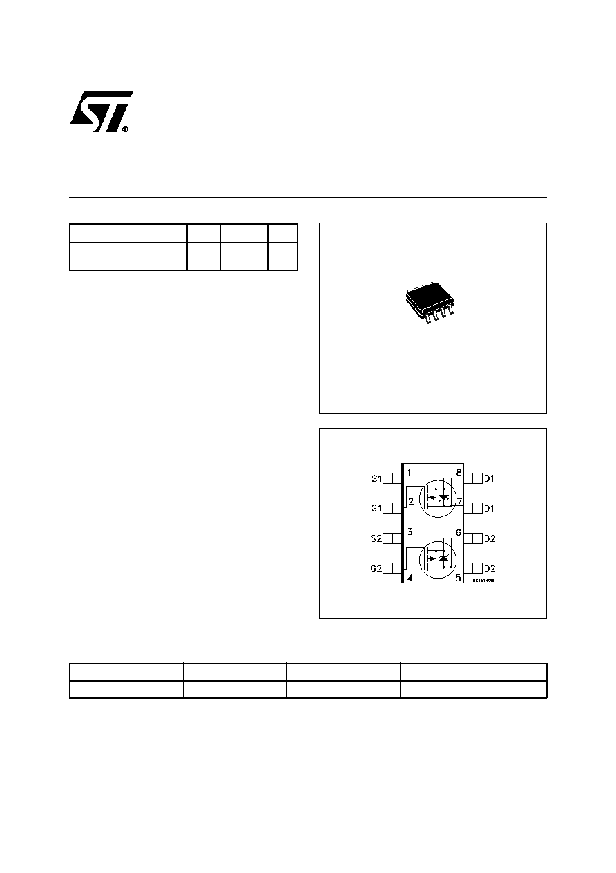
Figure 1: Package
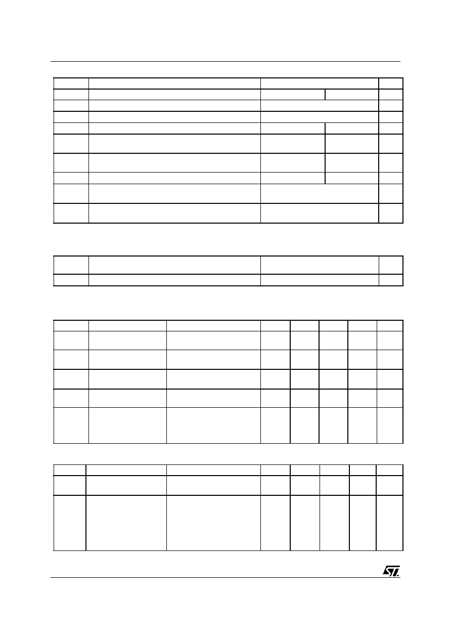
Figure 2: Internal Schematic Diagram
TYPE
V
DSS
R
DS(on)
I
D
STS8C5H30L (N-Channel)
STS8C5H30L (P-Channel)
30 V
30 V
< 0.022
< 0.055
8 A
5 A
SO-8
PART NUMBER
MARKING
PACKAGE
PACKAGING
STS8C5H30L
S8C5H30L
SO-8
TAPE & REEL
Rev. 2
STS8C5H30L
2/11
Table 3: Absolute Maximum ratings
( )
Pulse width limited by safe operating area
Note: For the P-CHANNEL MOSFET actual polarity of voltages and current has to be reversed
Table 4: Thermal Data
ELECTRICAL CHARACTERISTICS (T
CASE
=25∞C UNLESS OTHERWISE SPECIFIED)
Table 5: On/Off
Table 6: Dynamic
(1) Pulsed: Pulse duration = 300 µs, duty cycle 1.5%
Symbol
Parameter
Value
Unit
N-CHANNEL
P-CHANNEL
V
DS
Drain-source Voltage (V
GS
= 0)
30
V
V
DGR
Drain-gate Voltage (R
GS
= 20 k
)
30
V
V
GS
Gate- source Voltage
± 16
± 16
V
I
D
Drain Current (continuous) at T
C
= 25∞C
Single Operating
8
4.2
A
I
D
Drain Current (continuous) at T
C
= 100∞C
Single Operating
6.4
3.1
A
I
DM
( )
Drain Current (pulsed)
32
16.8
A
P
TOT
Total Dissipation at T
C
= 25∞C Dual Operating
Total Dissipation at T
C
= 25∞C Single Operating
1.6
2
W
W
T
j
T
stg
Operating Junction Temperature
Storage Temperature
150
-55 to 150
∞C
∞C
Rthj-case
Thermal Resistance Junction-case Single Operating
Dual Operating
62.5
78
∞C/W
∞C/W
T
l
Maximum Lead Temperature For Soldering Purpose
300
∞C
Symbol
Parameter
Test Conditions
Min.
Typ.
Max.
Unit
V
(BR)DSS
Drain-source
Breakdown Voltage
I
D
= 250 µA, V
GS
= 0
n-ch
p-ch
30
30
V
I
DSS
Zero Gate Voltage
Drain Current (V
GS
= 0)
V
DS
= Max Rating
V
DS
= Max Rating, T
C
= 125∞C
n-ch
p-ch
1
10
µA
µA
I
GSS
Gate-body Leakage
Current (V
DS
= 0)
V
GS
= ± 16V
V
GS
= ± 16V
n-ch
p-ch
±100
±100
nA
nA
V
GS(th)
Gate Threshold Voltage
V
DS
= V
GS
, I
D
= 250 µA
n-ch
p-ch
1
1
1.6
2.5
V
V
R
DS(on)
Static Drain-source On
Resistance
V
GS
= 10 V, I
D
= 4 A
V
GS
= 10 V, I
D
= 2.5 A
V
GS
= 4.5 V, I
D
= 4 A
V
GS
= 4.5 V, I
D
= 2.5 A
n-ch
p-ch
n-ch
p-ch
0.018
0.045
0.020
0.070
0.022
0.055
0.025
0.075
Symbol
Parameter
Test Conditions
Min.
Typ.
Max.
Unit
g
fs
(1)
Forward
Transconductance
V
DS
= 15 V
,
I
D
= 4 A
V
DS
= 15 V
,
I
D
= 2.5 A
n-ch
p-ch
8.5
10
S
S
C
iss
Input Capacitance
V
DS
= 25V, f = 1 MHz, V
GS
= 0
n-ch
p-ch
857
1350
pF
pF
C
oss
Output Capacitance
n-ch
p-ch
147
490
pF
pF
C
rss
Reverse Transfer
Capacitance
n-ch
p-ch
20
130
pF
pF
3/11
STS8C5H30L
ELECTRICAL CHARACTERISTICS(CONTINUED)
Table 7: Switching On
Table 8: Switching Off
Table 9: Source-Drain Diodef
(1) Pulsed: Pulse duration = 300 µs, duty cycle 1.5 %.
(2) Pulse width limited by safe operating area.
(3) C
oss eq.
is defined as a constant equivalent capacitance giving the same charging time as Coss when VDS increases from 0 to 80% VDSS
Symbol
Parameter
Test Conditions
Min.
Typ.
Max.
Unit
t
d(on)
t
r
Turn-on Delay Time
Rise Time
V
DD
= 15 V, I
D
= 4 A,
R
G
= 4.7
,
V
GS
= 4.5 V
P-CHANNEL
V
DD
= 15 V, I
D
= 2 A,
R
G
= 4.7
,
V
GS
= 4.5 V
(Resistive Load see, Figure 28)
n-ch
p-ch
n-ch
p-ch
12
25
14.5
35
ns
ns
ns
ns
Q
g
Total Gate Charge
V
DD
= 24 V, I
D
= 8 A,
V
GS
= 5 V
P-CHANNEL
V
DD
= 24 V, I
D
= 4 A,
V
GS
= 5 V
(see, Figure 31)
n-ch
p-ch
7
12.5
10
16
nC
nC
Q
gs
Gate-Source Charge
n-ch
p-ch
2.5
5
nC
nC
Q
gd
Gate-Drain Charge
n-ch
p-ch
2.3
3
nC
nC
Symbol
Parameter
Test Conditions
Min.
Typ.
Max.
Unit
t
d(off)
t
f
Turn-off Delay Time
Fall Time
V
DD
= 15 V, I
D
= 4 A,
R
G
= 4.7
,
V
GS
= 4.5 V
P-CHANNEL
V
DD
= 15 V, I
D
= 2.5 A,
R
G
= 4.7
,
V
GS
= 4.5 V
(Resistive Load see, Figure 28)
n-ch
p-ch
n-ch
p-ch
23
125
8
35
ns
ns
ns
ns
Symbol
Parameter
Test Conditions
Min.
Typ.
Max.
Unit
I
SD
Source-drain Current
n-ch
p-ch
8
5
A
A
I
SDM
(2)
Source-drain Current (pulsed)
n-ch
p-ch
32
20
A
A
V
SD
(1)
Forward On Voltage
I
SD
= 8 A, V
GS
= 0
I
SD
= 5 A, V
GS
= 0
n-ch
p-ch
1.5
1.2
V
V
t
rr
Reverse Recovery Time
I
SD
= 8 A, di/dt = 100 A/µs
V
DD
= 15V, T
j
= 150∞C
P-CHANNEL
I
SD
= 5 A, di/dt = 100 A/µs
V
DD
= 15V, T
j
= 150∞C
(see test circuit, Figure 29)
n-ch
p-ch
15
45
ns
ns
Q
rr
Reverse Recovery Charge
n-ch
p-ch
5.7
36
nC
nC
I
RRM
Reverse Recovery Current
n-ch
p-ch
0.76
1.6
A
A
STS8C5H30L
4/11
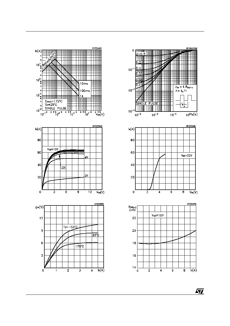
Figure 3:
.
Safe Operating n-channel
Figure 4: Output Characteristics n-channel
Figure 5: Transconductance n-channel
Figure 6: Thermal Impedance For Complemen-
tary Pair
Figure 7: Transfer Characteristics n-channel
Figure 8: Static Drain-Source On Resistance n-
channel
5/11
STS8C5H30L
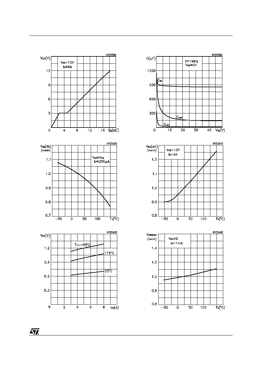
Figure 9: Gate Charge vs Gate-Source Voltage
n-channel
Figure 10: Normalized Gate Thereshold Volt-
age vs Temperature n-channel
Figure 11: Source-Drain Forward Characteris-
tics n-channel
Figure 12: Capacitance Variations n-channel
Figure 13: Normalized On Resistance vs Tem-
perature n-channel
Figure 14: Normalized BVdss vs Temperature
n-channel