April 2006
Rev 1
1/12
12
STC5DNF30V
Dual N-channel 30V - 0.032
- 4.5A - TSSOP8
2.7V-Driver STripFETTM Power MOSFET
General features
Standard outline for easy automated surface
mount assembly
Ultra low threshold gate drive (2.7V)
Description
This Power MOSFET is the latest development of
STMicroelectronics unique "Single Feature
SizeTM" strip-based process. The resulting
transistor shows extremely high packing density
for low on-resistance, rugged avalanche
characteristics and less critical alignment steps
therefore a remarkable manufacturing
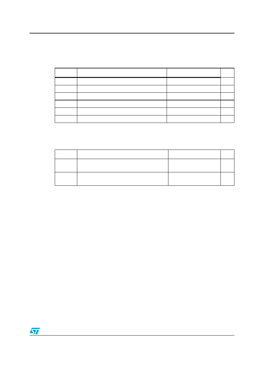
reproducibility. No electrical connections are
shared between mosfets.
Applications
Switching application
Internal schematic diagram
Type
V
DSS
R
DS(on)
I
D
STC5DNF30V
30V
< 0.035
(@4.5V)
< 0.040
(@2.7V)
4.5A
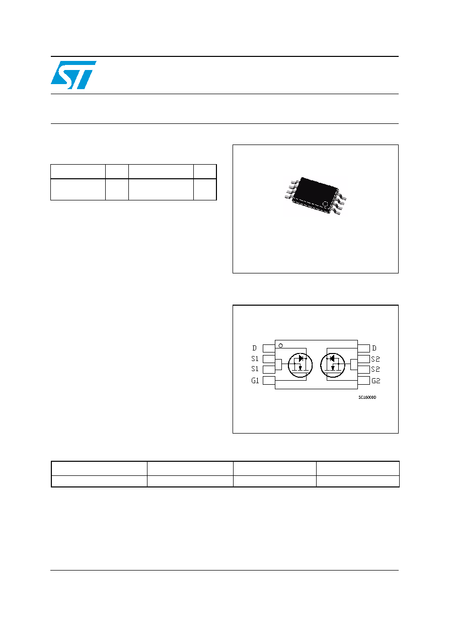
TSSOP8
www.st.com
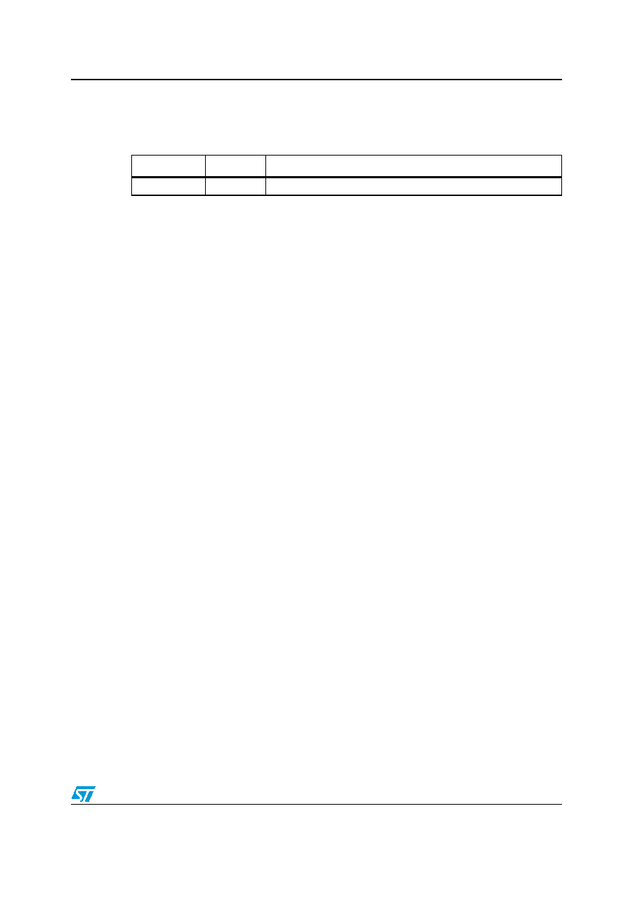
Order codes
Part number
Marking
Package
Packaging
STC5DNF30V
C5DNF30V
TSSOP8
Tape & reel

Contents
STC5DNF30V
2/12
Contents
1
Electrical ratings . . . . . . . . . . . . . . . . . . . . . . . . . . . . . . . . . . . . . . . . . . . . 3
2
Electrical characteristics . . . . . . . . . . . . . . . . . . . . . . . . . . . . . . . . . . . . . 4
2.1
Electrical characteristics (curves) . . . . . . . . . . . . . . . . . . . . . . . . . . . . . . . . 6
3
Test circuits . . . . . . . . . . . . . . . . . . . . . . . . . . . . . . . . . . . . . . . . . . . . . . 8
4
Package mechanical data . . . . . . . . . . . . . . . . . . . . . . . . . . . . . . . . . . . . . 9
5
Revision history . . . . . . . . . . . . . . . . . . . . . . . . . . . . . . . . . . . . . . . . . . . 11
STC5DNF30V
Electrical ratings
3/12
1 Electrical
ratings
Table 1.
Absolute maximum ratings
Symbol
Parameter
Value
Unit
V
DS
Drain-source voltage (V
GS
= 0)
30
V
V
GS
Gate- source voltage
± 8
V
I
D
(1)
1.
When mounted on FR-4 board with 1inch≤ pad, 2 Oz of Cu and t<10sec.
Drain current (continuous) at T
C
= 25∞C
4.5
A
I
D
(1)
Drain current (continuous) at T
C
= 100∞C
2.8
A
I
DM
(2)
2.
Pulse width limited by safe operating area
Drain current (pulsed)
18
A
P
TOT
(1)
Total dissipation at t
c
= 25∞C
1.3
W
Table 2.
Thermal data
Symbol
Parameter
Value
Unit
Rthj-pcb
(1)
Rthj-pcb
(2)
1.
When mounted on minimum recommended footprint.
2.
When mounted on FR-4 board with 1inch≤ pad, 2 Oz of Cu and t<10sec.
Thermal resistance junction-pcb max
Thermal resistance junction-pcb max
120
97.5
∞C/W
∞C/W
T
j
T
stg
Operating junction temperature
Storage temperature
-55 to 150
-55 to 150
∞C
∞C
Electrical characteristics
STC5DNF30V
4/12
2 Electrical
characteristics
(T
J
=25∞C unless otherwise specified)
Table 3.
On/off
Symbol
Parameter
Test conditions
Min.
Typ.
Max.
Unit
V
(BR)DSS
Drain-source
breakdown voltage
I
D
= 250µA, V
GS
= 0
30
V
I
DSS
Zero gate voltage
drain current
(V
GS
= 0)
V
DS
= Max rating
V
DS
= Max rating,T
C
=125∞C
1
10
µA
µA
I
GSS
Gate-body leakage
current (V
DS
= 0)
V
GS
= ± 8V
±100
nA
V
GS(th)
Gate threshold
voltage
V
DS
= V
GS
, I
D
= 250µA
0.6
V
R
DS(on)
Static drain-source on
resistance
V
GS
= 4.5V, I
D
= 2.3A
V
GS
= 2.7V, I
D
= 2.3A
0.032
0.036
0.035
0.040
Table 4.
Dynamic
Symbol
Parameter
Test conditions
Min.
Typ.
Max.
Unit
g
fs
Forward
transconductance
V
DS
=25V
;
I
D
= 2.3A
9.5
S
C
iss
C
oss
C
rss
Input capacitance
Output capacitance
Reverse transfer
capacitance
V
DS
= 25V, f = 1 MHz,
V
GS
= 0
460
200
50
pF
pF
pF
Q
g
Q
gs
Q
gd
Total gate charge
Gate-source charge
Gate-drain charge
V
DD
= 16V, I
D
= 4.5A,
V
GS
= 4.5V
(see Figure 14)
8.5
1.8
2.4
11.5
ns
ns
ns
Table 5.
Switching times
Symbol
Parameter
Test conditions
Min.
Typ.
Max.
Unit
t
d(on)
t
r
t
d(off)
t
r
Turn-on delay time
Rise time
Turn-off delay time
Fall time
V
DD
= 10V, I
D
= 2.3A,
R
G
= 4.7
V
GS
= 4.5V
(see Figure 13)
7
33
27
10
ns
ns
ns
ns
t
r(Voff)
t
f
t
c
Off-voltage rise time
Fall time
Cross-over time
V
DD
= 16V, I
D
= 2.3A,
R
G
= 4.7
,
V
GS
= 4.5V
(see Figure 17)
26
11
21
ns
ns
ns
STC5DNF30V
Electrical characteristics
5/12
Table 6.
Source drain diode
Symbol
Parameter
Test conditions
Min.
Typ.
Max.
Unit
I
SD
I
SDM
(1)
1.
Pulse width limited by safe operating area.
Source-drain current
Source-drain current
(pulsed)
4.5
18
A
A
V
SD
(2)
2.
Pulsed: Pulse duration = 300 µs, duty cycle 1.5 %.
Forward on voltage
I
SD
= 4.5A, V
GS
= 0
1.2
V
t
rr
Q
rr
I
RRM
Reverse recovery time
Reverse recovery charge
Reverse recovery current
I
SD
= 4.5A, di/dt =100A/µs,
V
DD
= 10V, T
j
= 150∞C
(see Figure 15)
26
13
1
ns
nC
A
Electrical characteristics
STC5DNF30V
6/12
2.1
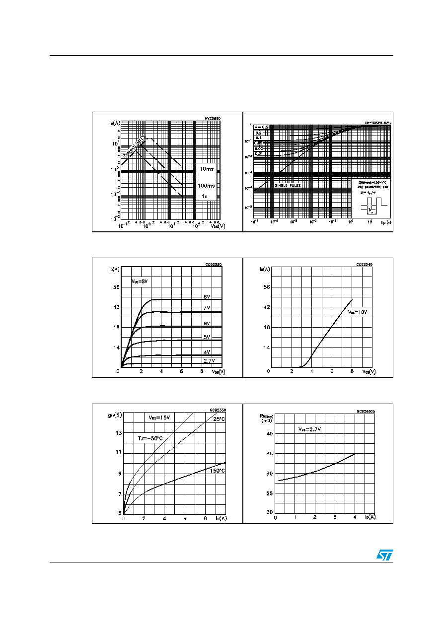
Electrical characteristics (curves)
Figure 1.
Safe operating area
Figure 2.
Thermal impedance
Figure 3.
Output characteristics
Figure 4.
Transfer characteristics
Figure 5.
Transconductance
Figure 6.
Static drain-source on
resistance
STC5DNF30V
Electrical characteristics
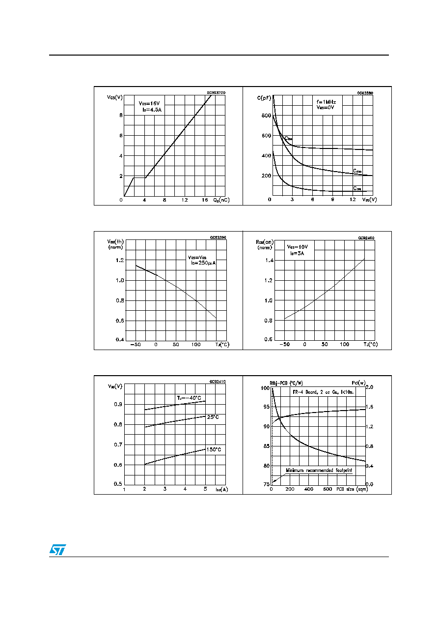
7/12
Figure 7.
Gate charge vs gate-source
voltage
Figure 8.
Capacitance variations
Figure 9.
Normalized gate thereshold
voltage vs temperature
Figure 10. Normalized on resistance vs
temperature
Figure 11. Source-drain diode forward
characteristics
Figure 12. Thermal resistance and max
power
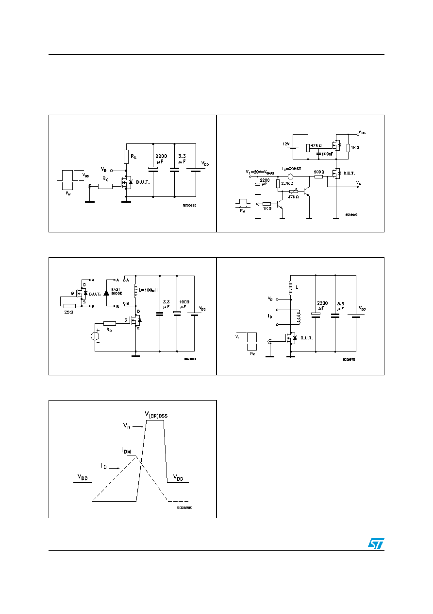
Test circuits
STC5DNF30V
8/12
3
Test circuits
Figure 13. Switching times test circuit for
resistive load
Figure 14. Gate charge test circuit
Figure 15. Test circuit for inductive load
switching and diode recovery times
Figure 16. Unclamped inductive load test
circuit
Figure 17. Unclamped inductive waveform

STC5DNF30V
Package mechanical data
9/12
4 Package
mechanical
data
In order to meet environmental requirements, ST offers these devices in ECOPACKÆ
packages. These packages have a Lead-free second level interconnect . The category of
second level interconnect is marked on the package and on the inner box label, in
compliance with JEDEC Standard JESD97. The maximum ratings related to soldering
conditions are also marked on the inner box label. ECOPACK is an ST trademark.
ECOPACK specifications are available at:
www.st.com
Package mechanical data
STC5DNF30V
10/12
DIM.
mm.
inch
MIN.
TYP
MAX.
MIN.
TYP.
MAX.
A
1.05
1.20
0.041
0.047
A1
0.05
0.15
0.002
0.006
A2
0.80
1.05
0.032
0.041
b
0.19
0.30
0.008
0.012
c
0.127
0.005
D
2.90
3.10
0.114
0.122
E
4.30
4.50
0.170
0.177
E1
6.20
6.60
0.240
0.260
E2
5.14
5.24
0.202
0.206
e
0.65
0.025
L
0.45
0.75
0.018
0.030
L1
0.90
1.10
0.0355
0.0433
R
0.09
0.004
R1
0.09
0.004
1
0
∞
8
∞
0
∞
8
∞
2
12
∞
TSSOP8 MECHANICAL DATA
STC5DNF30V
Revision history
11/12
5 Revision
history
Table 7.
Date
Revision
Changes
11-Apr-2006
1
First release

STC5DNF30V
12/12
Please Read Carefully:
Information in this document is provided solely in connection with ST products. STMicroelectronics NV and its subsidiaries ("ST") reserve the
right to make changes, corrections, modifications or improvements, to this document, and the products and services described herein at any
time, without notice.
All ST products are sold pursuant to ST's terms and conditions of sale.
Purchasers are solely responsible for the choice, selection and use of the ST products and services described herein, and ST assumes no
liability whatsoever relating to the choice, selection or use of the ST products and services described herein.
No license, express or implied, by estoppel or otherwise, to any intellectual property rights is granted under this document. If any part of this
document refers to any third party products or services it shall not be deemed a license grant by ST for the use of such third party products
or services, or any intellectual property contained therein or considered as a warranty covering the use in any manner whatsoever of such
third party products or services or any intellectual property contained therein.
UNLESS OTHERWISE SET FORTH IN ST'S TERMS AND CONDITIONS OF SALE ST DISCLAIMS ANY EXPRESS OR IMPLIED
WARRANTY WITH RESPECT TO THE USE AND/OR SALE OF ST PRODUCTS INCLUDING WITHOUT LIMITATION IMPLIED
WARRANTIES OF MERCHANTABILITY, FITNESS FOR A PARTICULAR PURPOSE (AND THEIR EQUIVALENTS UNDER THE LAWS
OF ANY JURISDICTION), OR INFRINGEMENT OF ANY PATENT, COPYRIGHT OR OTHER INTELLECTUAL PROPERTY RIGHT.
UNLESS EXPRESSLY APPROVED IN WRITING BY AN AUTHORIZE REPRESENTATIVE OF ST, ST PRODUCTS ARE NOT DESIGNED,
AUTHORIZED OR WARRANTED FOR USE IN MILITARY, AIR CRAFT, SPACE, LIFE SAVING, OR LIFE SUSTAINING APPLICATIONS,
NOR IN PRODUCTS OR SYSTEMS, WHERE FAILURE OR MALFUNCTION MAY RESULT IN PERSONAL INJURY, DEATH, OR
SEVERE PROPERTY OR ENVIRONMENTAL DAMAGE.
Resale of ST products with provisions different from the statements and/or technical features set forth in this document shall immediately void
any warranty granted by ST for the ST product or service described herein and shall not create or extend in any manner whatsoever, any
liability of ST.
ST and the ST logo are trademarks or registered trademarks of ST in various countries.
Information in this document supersedes and replaces all information previously supplied.
The ST logo is a registered trademark of STMicroelectronics. All other names are the property of their respective owners.
© 2006 STMicroelectronics - All rights reserved
STMicroelectronics group of companies
Australia - Belgium - Brazil - Canada - China - Czech Republic - Finland - France - Germany - Hong Kong - India - Israel - Italy - Japan -
Malaysia - Malta - Morocco - Singapore - Spain - Sweden - Switzerland - United Kingdom - United States of America
www.st.com