1/15
January 2005
I
SUB-LOW VOLTAGE DIFFERENTIAL
SIGNALING INPUTS:
V
ID
= 100mV WITH R
T
= 100
, C
L
=10pF
I
V
TH
=±25mV WITH R
T
=100
,
C
L
=10pF
I
HIGH SIGNALING RATE:
f
IN
= 416MHz MAX (D+,D-,CLK+,CLK-)
f
OUT
= 52 MHz MAX (D1-D8,CLK)
I
VERY HIGH SPEED:
t
pLH
~t
pHL
=3.5ns (TYP) at V
DD
=2.8V; V
L
=1.8V
I
OPERATING VOLTAGE RANGE:
V
DD
(OPR) = 2.65V to 3.6V
V
L
(OPR) =1.65V to 1.95V
I
SYMMETRICAL OUTPUT IMPEDANCE
(D1-D8, H-SYNC, V-SYNC, CLK):
II
OH
I= I
OL
=8mA (MIN) at V
DD
=2.65V;V
L
=1.8V
I
LOW POWER DISSIPATION
(DISABLED: EN=Gnd):
I
SOFF
=I
DD
+ I
L
= 10
µ
A (Max)
I
CMOS LOGIC INPUT THRESHOLD
(EN, SYNC_SEL):
V
IL
= 0.3xV
DD
; V
DD
=2.65V to 3.6V
V
IH
= 0.7xV
DD
; V
DD
=2.65V to 3.6V
I
BIDIRECTIONAL LEVEL TRANSLATOR LINE
(I/O
VDD
, I/O
VL
) FOR I
2
C COMMUNICATIONS:
13Mbps MAX DATA RATE
II
OH
I= 20
µ
A (MIN.) at V
DD
=2.8V;V
L
=1.8V
I
OL
= 1 mA (MIN.) at V
DD
=2.8V;V
L
=1.8V
I
3.6V TOLERANT on INPUTS
(EN, SYNC_SEL)
I
LEADFREE
µ
TFBGA PACKAGE
(RoHS Restriction of Hazardous Substances)
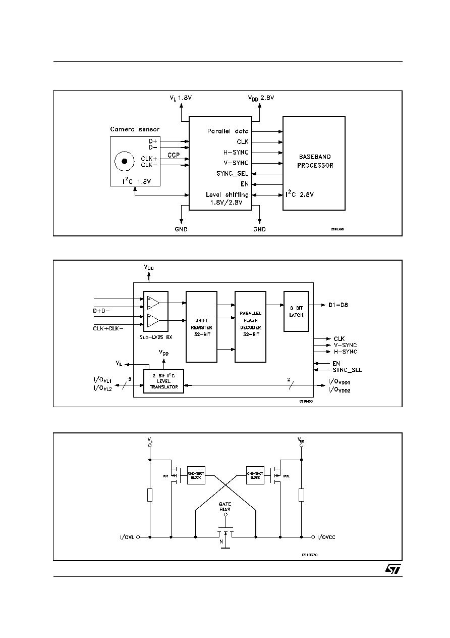
DESCRIPTION
The STCCP27 receiver converts the SubLVDS
clock/datastream (up to 416 Mbps throughput
bandwidth) back into parallel 8 bits of CMOS/
LVTTL. The device recognizes the CCP 32bit start
of frame (SOF), end of frame (EOF), start of line
(SOL) and end of line (EOL) sequences to
generate the H-SYNC and V-SYNC signals.
Output LVTTL clock (up to 52 MHz) is transmitted
in parallel with data. Input and Output data are
rising edge strobe. This chipset is an ideal means
to link mobile camera modules to baseband
processors. In order to minimize static current
consumption, it is possible to shut down the
device when the interface is not being used by a
power-down (EN) pin that reduces to 10
µ
A the
Maximum Current Consumption making this
device ideal for portable applications like Mobile
Phone, Portable Battery Equipment.
Two dedicated I
2
C lines are provided to translate
bidirectional controls from camera and
µ
C
devices. The STCCP27 is offered in a
µ
TFBGA
package to optimize PCB space.
All inputs and outputs are equipped with
protection circuits against static discharge, giving
them ESD immunity from transient excess
voltage. The STCCP27 is characterized for
operation over the commercial temperature range
-40∞C to 85∞C.
Table 1: Order Codes
Type
Temperature
Range
Package
Comments
STCCP27TBR
-40 to 85 ∞C
µTFBGA25 3x3mm (TAPE & REEL)
3000 parts per reel
STCCP27
1.8 HIGH SPEED DUAL DIFFERENTIAL LINE RECEIVERS,
COMPACT CAMERA PORT DECODER, I
2
C CONTROL LINE
This is preliminary information on a new product now in development. Details are subject to change without notice.
µTFBGA25
PRODUCT PREVIEW
Rev. 1
STCCP27
4/15
Table 3: Main Function Table
Z = High Impedance, L = Low Voltage Level, H = High Voltage Level, X = Don't care
Table 4: I
2
C Bus Function Table
Open: If I/O
VDD
is not driven then the I/O
VL
will go in high level V
L
by embedded 10k
pull-up resistor; If I/O
VL
is not driven then the I/O
VCC
will go in high
level V
DD
by embedded 10K
pull-up resistor
Figure 5: Frame Structure In VGA Case (Allowed Synchronization Codes Sequence)
INPUT
OUTPUT
FUNCTION
ENABLE
SYNC_SEL
D+
D-
CLK+ CLK-
V-SYNC
H-SYNC
D1-D8
CLK
L
X
X
X
X
X
L
L
L
L
CCP disabled
H
H
SOF (FF
H
00
H
00
H
02
H
)
H
H
See Detailed
Timing Diagram
Start of Frame
H
H
EOF(FF
H
00
H
00
H
03
H
)
L
L
End of Frame
H
H
SOL(FF
H
00
H
00
H
00
H
)
No Change
H
Start of Line
H
H
EOL(FF
H
00
H
00
H
01
H
)
No Change
L
End of Line
H
L
X
X
X
X
L
L
D+, D-
See
Detailed
Timing
Diagram
Disabled Sync
(D1-D8 will get
out data, includ-
ing Sync Code)
ENABLE
I/O INPUT
FUNCTION
I/O
VDD
I/O
VL
X
L
L
I
2
C Comm.
X
V
DD
V
L
I
2
C Comm.
X
Open
V
L
I
2
C Comm.
X
V
DD
Open
I
2
C Comm.

STCCP27
5/15
Table 5: Absolute Maximum Ratings
Absolute Maximum Ratings are those values beyond which damage to the device may occur. Functional operation under these condition is
not implied.
Table 6: Recommended Operating Conditions
Symbol
Parameter
Value
Unit
V
DD
Main Supply Voltage
-0.5 to 4.6
V
V
L
Secondary Supply Voltage
-0.5 to 4.6
V
V
D
SubLVDS Data Bus Input Voltage (D+, D-)
-0.5 to 4.6
V
V
CLK
SubLVDS Clock Bus Input Voltage (CLK+, CLK-)
-0.5 to 4.6
V
V
I
DC Input Voltage (SYNC_SEL, EN)
-0.5 to 4.6
V
V
O
DC Output Voltage (D1-D8, H-SYNC, V-SYNC, CLK, I/O
VDD
)
-0.5 to (V
DD
+ 0.5)
V
V
I/OVL
DC Output Voltage (I/O
VL
)
-0.5 to (V
L
+ 0.5)
V
T
stg
Storage Temperature Range
-65 to +150
∞C
ESD
Electrostatic Discharge Protection
HBM Human Body Model (All Pins)
±2
KV
Symbol
Parameter
Min.
Typ.
Max.
Unit
V
DD
Main Supply Voltage
2.65
2.8
3.6
V
V
L
Secondary Supply Voltage
1.65
1.8
1.95
V
V
ID
Differential Level Input Voltage (D+, D-, CLK1+, CLK1-)
0.1
0.4
V
V
CM
Common Level Input Voltage (D+, D-, CLK1+, CLK1-)
0.5
0.9
1.3
V
V
IC
Level Input Voltage (SYNC_SEL, EN)
3.6
V
V
I/OVDD
Level Input Voltage (I/O
VDD
)
V
DD
V
V
I/OVL
Level Input Voltage (I/O
VL
)
V
L
V
R
T
Termination Resistance (per pair differential input line)
80
100
120
C
L
Termination Capacitance (per line vs Gnd Pin)
10
pF
T
A
Operating Ambient Temperature Range
-40
85
∞C
T
J
Operating Junction Temperature Range
-40
125
∞C
t
R
, t
F
Rise and Fall Time
(SYNC_SEL, EN, I/O
VDD
, I/O
VL
; 10% to 90%; 90% to
10%)
10
ns