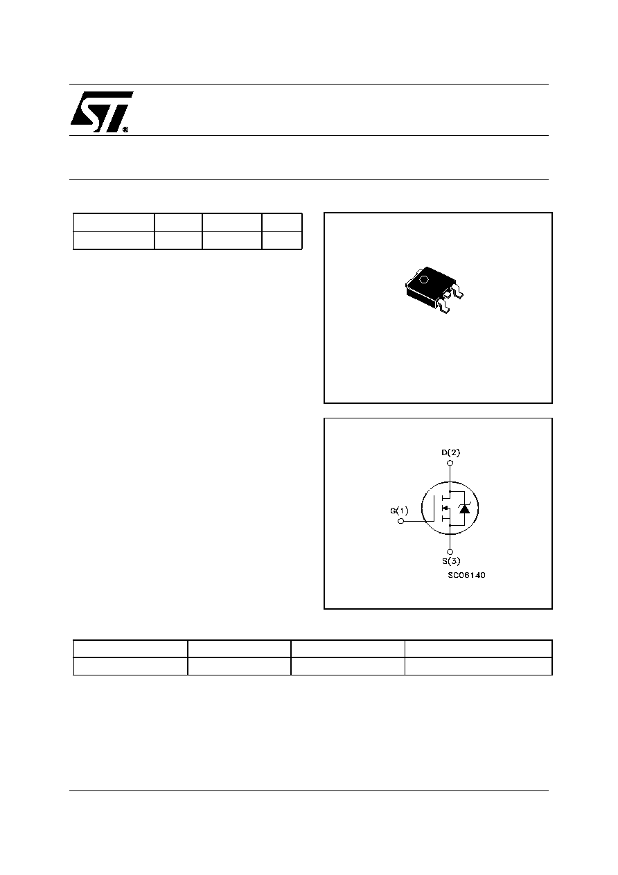
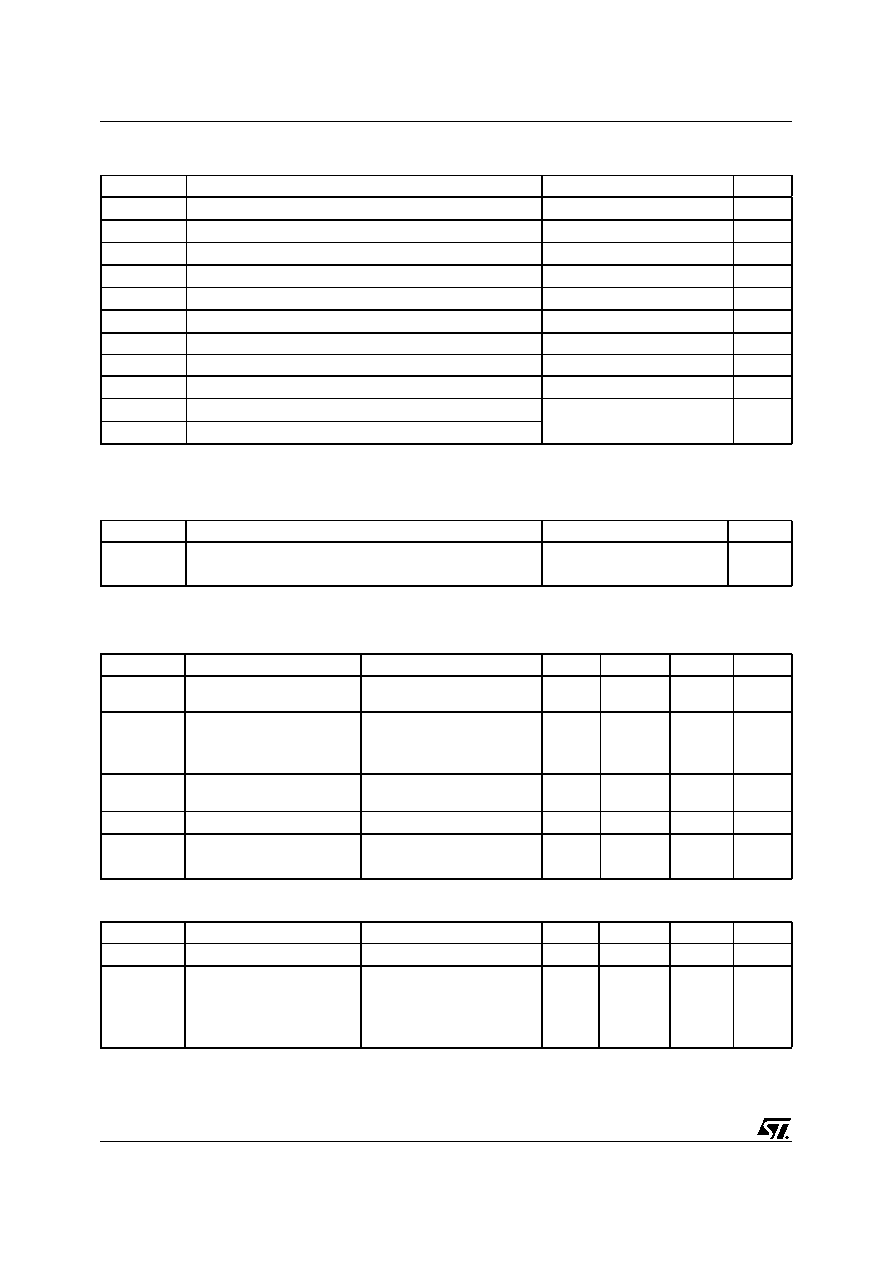
N-CHANNEL 55V 0.012Ohm 60A DPAK STripFET II MOSFET
1/11
February 2005
STD60NF55LA
N-CHANNEL 55V - 0.012
- 60A DPAK
STripFETTMII MOSFET
Table 1: General Features
s
TYPICAL R
DS(on)
= 0.012
s
LOW THRESHOLD DRIVE
DESCRIPTION
This MOSFET is the latest development of STMi-
croelectronics unique "Single Feature Size
TM"
strip-based process. The resulting transistor
shows extremely high packing density for low on-
resistance, rugged avalance characteristics and
less critical alignment steps therefore a remark-
able manufacturing reproducibility.
APPLICATIONS
s
HIGH CURRENT, HIGH SWITCHING SPEED
Table 2: Order Codes
Figure 1: Package
Figure 2: Internal Schematic Diagram
TYPE
V
DSS
R
DS(on)
I
D
(1)
STD60NF55LA
55V
< 0.015
60A
DPAK
1
3
Part Number
Marking
Package
Packaging
STD60NF55LAT4
D60NF55LA
DPAK
TAPE & REEL
Rev. 1
STD60NF55LA
2/11
Table 3: Absolute Maximum ratings
(
q
) Pulse width limited by safe operating area
(1)I
SD
40A, di/dt
350A/�s, V
DD
V
(BR)DSS
, T
j
T
JMAX.
(2) Starting T
j
=25�C, I
D
=30A, V
DD
=20V
Table 4: Thermal Data
ELECTRICAL CHARACTERISTICS (T
CASE
=25�C UNLESS OTHERWISE SPECIFIED)
Table 5: On /Off
Table 6: Dynamic
Symbol
Parameter
Value
Unit
V
DS
Drain-source Voltage (V
GS
= 0)
55
V
V
GS
Gate- source Voltage
� 15
V
I
D
Drain Current (continuous) at T
C
= 25�C
60
A
I
D
Drain Current (continuous) at T
C
= 100�C
42
A
I
DM
( )
Drain Current (pulsed)
240
A
P
TOT
Total Dissipation at T
C
= 25�C
110
W
Derating Factor
0.73
W/�C
dv/dt (1)
Peak Diode Recovery voltage slope
16
V/ns
E
AS
(2)
Single Pulse Avalanche Energy
400
mJ
T
stg
Storage Temperature
� 55 to 175
�C
T
j
Operating Junction Temperature
Rthj-case
Thermal Resistance Junction-case Max
1.36
�C/W
Rthj-amb
Thermal Resistance Junction-ambient Max
62.5
�C/W
T
l
Maximum Lead Temperature For Soldering Purpose
275
�C
Symbol
Parameter
Test Conditions
Min.
Typ.
Max.
Unit
V
(BR)DSS
Drain-source
Breakdown Voltage
I
D
= 250 �A, V
GS
= 0
55
V
I
DSS
Zero Gate Voltage
Drain Current (V
GS
= 0)
V
DS
= Max Rating
1
�A
V
DS
= Max Rating,
T
C
= 125�C
10
�A
I
GSS
Gate-body Leakage
Current (V
DS
= 0)
V
GS
= � 15 V
�100
nA
V
GS(th)
Gate Threshold Voltage
V
DS
= V
GS
, I
D
= 250�A
1
2
V
R
DS(on)
Static Drain-source On
Resistance
V
GS
= 10 V, I
D
= 30 A
0.012
0.015
V
GS
= 5 V, I
D
= 30 A
0.014
0.017
Symbol
Parameter
Test Conditions
Min.
Typ.
Max.
Unit
g
fs
(1)
Forward Transconductance
V
DS
= 10
V, I
D
= 30 A
35
S
C
iss
Input Capacitance
V
DS
= 25V, f= 1 MHz, V
GS
= 0
1950
pF
C
oss
Output Capacitance
390
pF
C
rss
Reverse Transfer
Capacitance
130
pF
3/11
STD60NF55LA
ELECTRICAL CHARACTERISTICS (CONTINUED)
Table 7: Switching On
Table 8: Switching
Table 9: Source Drain Diode
(1) Pulsed: Pulse duration = 300 �s, duty cycle 1.5 %.
(2) Pulse width limited by safe operating area.
Symbol
Parameter
Test Conditions
Min.
Typ.
Max.
Unit
t
d(on)
Turn-on Delay Time
V
DD
= 25 V, I
D
= 30 A
R
G
= 4.7
V
GS
= 4.5V
(see test circuit, Figure 3)
30
ns
t
r
Rise Time
180
ns
Q
g
Q
gs
Q
gd
Total Gate Charge
Gate-Source Charge
Gate-Drain Charge
V
DD
= 40 V, I
D
= 60 A,
V
GS
= 5 V
40
10
20
nC
nC
nC
Symbol
Parameter
Test Conditions
Min.
Typ.
Max.
Unit
t
d(off)
t
f
Turn-off-Delay Time
Fall Time
V
DD
= 25 V, I
D
= 30 A,
R
G
= 4.7
,
V
GS
= 4.5V
(see test circuit, Figure 3)
80
35
ns
ns
Symbol
Parameter
Test Conditions
Min.
Typ.
Max.
Unit
I
SD
Source-drain Current
60
A
I
SDM
(2)
Source-drain Current (pulsed)
240
A
V
SD
(1)
Forward On Voltage
I
SD
= 60A, V
GS
= 0
1.3
V
t
rr
Q
rr
I
RRM
Reverse Recovery Time
Reverse Recovery Charge
Reverse Recovery Current
I
SD
= 40 A, di/dt = 100 A/�s, V
DD
= 25 V, T
j
= 150 �C
(see test circuit, Figure 5)
65
130
4
ns
nC
A
STD60NF55LA
4/11
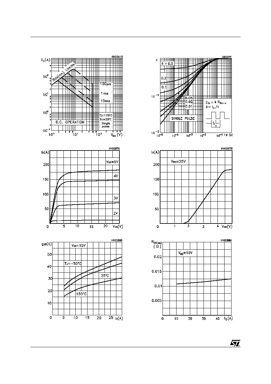
Figure 3: Safe Operating Area
Figure 4: Output Characteristics
Figure 5: Transconductance
Figure 6: Thermal Impedance
Figure 7: Transfer Characteristics
Figure 8: Static Drain-source On Resistance
5/11
STD60NF55LA
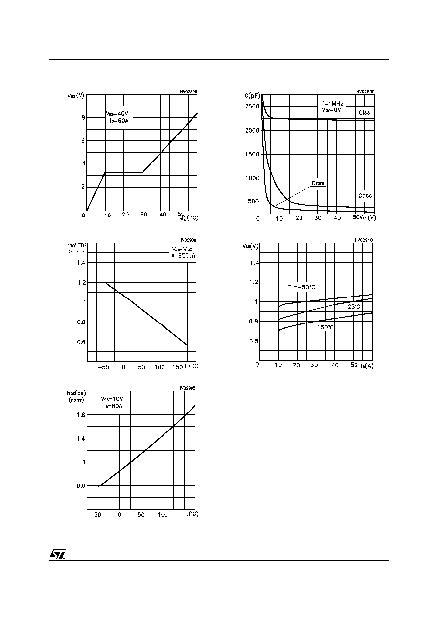
Figure 9: Gate Charge vs Gate-source Voltage
Figure 10: Normalized Gate Thereshold Volt-
age vs Temperature
Figure 11: Normalized On Resistance vs Tem-
perature
Figure 12: Capacitance Variation
Figure 13: Source-Drain Diode Forward Char-
acteristics
Document Outline